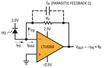
Photodiodes are used in a wide variety of applications to transform light into a current or voltage. These range from solar cells to optical data networks, from precision instruments to chromatography to medical imaging. All of these applications share a need for circuitry to buffer and scale the photodiode output. For applications requiring high speed and high dynamic range, transimpedance amplifier (TIA) circuits like the one shown in Fig. 1 are often used. In this figure, the feedback capacitance is shown as parasitic. For many applications, this is a deliberately placed capacitor to ensure stability.

Fig. 1: The transimpedance amplifier.
This circuit has the photodiode in “photoconductive mode” with a bias voltage applied to the cathode. The virtual connection between the two op amp inputs holds the anode at ground, thus applying a constant reverse bias voltage across the photodiode. A photodiode can be thought of as a current source (proportional to light intensity), a capacitor, a large resistor, and a so-called dark current – all connected in parallel.
The larger the bias voltage across the photodiode, the smaller the device's capacitance becomes. While this is good for speed, it is limited in practice by the capability of a photodiode to withstand large reverse voltages.
Circuit operation
The current generated by the photodiode (IPD) is amplified by the TIA circuit and converted to an output voltage through the transimpedance gain resistor (also referred to as the feedback resistor, or RF ). Ideally all of this current flows through RF (i.e., IFB = IPD ), but in practice the amplifier “steals” some of this current in the form of input bias current. This bias current results in an error voltage at the output and limits dynamic range. The larger the gain resistor, the greater this effect. It is important to select an amplifier with sufficiently low bias current (as well as input offset voltage and offset voltage drift) to achieve the required dynamic range and overall accuracy.
One other consideration is the effect of op amp input current variation over temperature. Op amps with bipolar input stages have fairly constant input current. But this current is so high even at room temperature (nA or even µA) that unbuffered bipolar amplifiers are not suitable for many high transimpedance gain applications. For this reason, op amps with a FET input stage are preferred because they have inherently lower input current — often in the single digit picoampere range or even lower at room temperature.
But, input ESD protection diodes leak as they get hot, causing the input current to rise exponentially with temperature. It is not unusual for an op amp with pA bias current at room temperature to have nA input current at 125°C. An op amp that addresses this problem by bootstrapping the ESD diodes is described later in this article. Another alternative is to use a discrete FET to buffer the photodiode at the amplifier input, but this requires an additional component and the associated board space and has relatively high input capacitance.

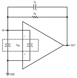
Fig. 2: Input capacitance includes sensor, board, and amplifier capacitance.
Since dynamic range is the ratio of maximum output signal to noise, it is also important to select an op amp with sufficiently low noise. Op amp current noise and voltage noise both matter, in varying degrees depending on the value of RF and CIN . The input capacitance, CIN (see Fig. 2 ), is a combination of the photodiode capacitance, the amplifier input capacitance, and stray board capacitances. In transimpedance amplifier circuits, the current noise is multiplied by RF , causing noise to appear as an output voltage error. Also, the amplifier’s voltage noise is multiplied by the noise gain. So for higher RF values, current noise (in) becomes more dominant, and for circuits with high CIN , voltage noise (en ) dominates. Finding an op amp with both low current noise and low voltage noise can be challenging.
Input capacitance also limits bandwidth. One way to think about this is to consider the impedance of the input capacitor as the gain resistor (RG ) in a conventional inverting op amp configuration. The larger the capacitor, the smaller the impedance and the larger the effective gain the op amp “sees” (1+RF /RG ), often called the noise gain. Since an amplifier’s bandwidth is inversely proportional to gain due to the constant nature of the gain-bandwidth product, this means that a large input capacitance limits the circuit bandwidth.
This can also be thought of in terms of stability. Capacitance at an op amp input can create a pole in the frequency domain or a lag in the time domain. This pole can be compensated to make the circuit stable by adding a feedback capacitor (CF ). The larger this capacitance, the more limited the circuit bandwidth. Thus it is important to choose an amplifier with low input capacitance and to carefully lay out the board to avoid stray input capacitance and feedback capacitance. See pages 14 and 15 of the LTC6268 datasheet for some practical ideas for reducing stray feedback capacitance which in practice achieves greater than 4x improvement in circuit bandwidth.
Available amplifiers
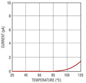
There are a number of extremely low-input-bias amps available — some with bias as low as 40 fA at room temperature. One excellent example is our new LTC6268 femtoamp bias current op amp — an amplifier has the low bias along with the performance required by high speed, high dynamic range photodiode circuits described in this article. It achieves extremely low input current by bootstrapping the on-chip ESD protection diodes. By creating a buffered replica of the input voltage and feeding that into split ESD diodes, diode voltage and current are kept extremely low during normal operation. The result is guaranteed max input bias current of 0.9 pA at 85°C and 4 pA at 125°C. Bias current at room temperature is typically only 3 fA. Typical input current performance is shown in Fig. 3 . While this current still increases over temperature, it is orders of magnitude lower than that of other amplifiers.

Fig. 3: LTC6268 input bias current remains low over temperature.
The LTC6268 has 500-MHz gain bandwidth, enabling the single-stage circuits, as shown in the device datasheet, that have 20 kΩ transimpedance gain with 65 MHz bandwidth or 499-kΩ transimpedance gain with 11.2 MHz bandwidth. With just 0.45-pF common-mode input capacitance, the amplifier contributes only a small portion of the total circuit capacitance, preserving high bandwidth. The input referred voltage and current noise of the device is 4.3 nV/√Hz at 1 MHz and 5.5 fA/√Hz at 100 kHz, respectively. Its wide bandwidth, low distortion, and high slew rate makes it suitable for high speed digitizing applications.
Although hundreds, if not thousands, of op amps are available on the market, finding a suitable transimpedance amp for high speed, high dynamic range photodiode circuits can be very challenging. Each requires its own unique combination of performance characteristics, including extremely low input bias current and input current temperature drift, high speed (e.g., gain bandwidth product and slew rate), the right balance of low voltage and current noise, and low input capacitance.
Advertisement
Learn more about Linear Technology


