Quality testing of PCBs ensures all aspects of a design are correctly implemented and end products perform exactly as expected. While testing does not necessarily deliver quality – which is a design issue – quality testing often includes:
– A check of the design rules to verify the design is free of layout errors,
– Electrical testing to quality check the inner layers of the PCB, and
– Optical inspection to discover violations of line width and spacing or even hole breakage.
Given mixed-performance requirements, today’s PCBs are amazingly complex. They also typically feature a diverse set of highly sensitive components, and they are quite literally crammed with capabilities on shrinking real estate. For these reasons, quality testing for component compatibility and manufacturability is critical, especially during the prototype stage when speed and flexibility are a must.
Quality inspection and testing are performed to standards set by customers based on the predicted use of the end product. For example, an IPC-A-600 standard inspection describes the preferred, acceptable and non-conforming conditions externally or internally observable on PCBs. UL inspections may be required should there be potential for product flammability.
While there are many testing methods, visual inspection is at the top of the list. How does the PCB look? What is obvious to the trained eye? Visual checks along the way include checking solder-mask ink coating, surface-finish thickness, adhesion, and copper removal, among others.
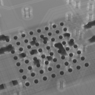
However, sometimes it takes more than visual inspection to ensure the quality of the PCB so inspection tools that specifically target PCB-assembly quality are often used. For example, the X-Tek “Revolution” X-ray Inspection System can verify the quality of ball-grid-array (BGA) components and analyze solder-ability conditions on IC packages and connectors. Using computed-tomography (CT) inspection, the system reconstructs a test sample in full-3D imagery, providing high-resolution magnification that unearths problems impossible to discover using the naked eye.
Another testing method is automatic optical inspection (AOI), which scans a device under test (DUT) for surface-feature defects including scratches and stains, thinning of the solder, missing or incorrect components, and incorrect component placement. In addition, inner-layer copper patterns are scanned and compared with design data so that no open or short circuits exist to cause malfunctions.
Flying-probe test systems also are used for basic production, prototypes, and boards in which accessibility is an issue. In these test systems, electromechanically controlled probes access analog components, analog signatures, and short or open circuits, probing points without the use of expensive fixtures or programming.
Since SMT components are often smaller than their through-hole counterparts because of smaller leads or no leads, verification software is used to find errors before assembly begins.
Quality testing based on specifications and design criteria is a necessity and must span many processes to mitigate potential end-product technical issues.
For more information, visit the Advanced Assembly website.
Advertisement
Learn more about Advanced Assembly


