Embedded applications are constantly evolving to become smarter and include more features. This demand means microcontrollers need more processing capabilities to crunch data faster and more efficiently, more intelligent peripherals to sample or transfer data faster and more accurately, and more interaction with external components or systems. High performance requirements translate into a more power-hungry embedded system. On the other hand, the industry also demands embedded systems with lower power. This means applications need longer lifetimes on existing power budgets or smaller power sources for light-weight or cost-sensitive applications. Some applications even depend entirely on renewable or energy-harvesting resources. These two contradicting requirements create a challenge for embedded developers to push the envelope of innovation.
The geometric progression
A large number of MCUs on the market today are on larger process nodes (230 or 180 nm) to leverage low manufacturing cost and low-leakage benefits for low- to medium-performance applications with relatively low complexity and processing speed (
For applications needing higher processing capabilities, silicon manufacturers have continued to invest in newer and smaller process node technologies. Smaller geometries enable higher performance CPUs with higher gate counts, pack in more memory or add more peripherals to the chip configuration without jeopardizing cost. Smaller process nodes also enable higher processing speeds at reasonable power consumption. For ultra-low-power MCUs, CPU frequency of 48 MHz or higher with acceptable active power consumption can be realized at the 90 nm process node and smaller. However, MCU vendors still need to make optimizations to reduce active current consumption at these nodes.
The downside of smaller geometries is increased leakage current. This is especially detrimental applications where a system only periodically wakes to perform a task and spends most of its life at sleep. Increasing the leakage current can have a proportional impact to the device’s power budget or battery lifetime. The leakage current is not only impacted by the process technology but also the size of the chip or the total gate count. This poses a number of problems that need to be solved, starting with semiconductor manufacturers.
Minimizing energy consumption in high-performance MCUs
Silicon manufacturers can put in a lot of innovation and differentiation into lowering power consumption. There are two problems that require completely different solutions: active and sleep (leakage) currents.
Decreasing power, execution time, or both, reduces energy. Minimizing the operating voltage naturally reduces power consumption. On some MCUs, increasing the operating frequencies might require a higher minimum supply voltage, while more robust MCUs can support operation across the frequency range at any supply voltage in their range. It has become very common for MCUs to have a second voltage rail, much lower than VCC, for the internal CPU core and digital logics (VCORE). Since these components operate at higher frequency and consume more current, restricting them at a lower voltage could result in additional power savings. Depending on the range of the MCU operating frequency, it might be beneficial to break down to smaller ranges and introduce multiple core voltage levels to further throttle the power output for each frequency range.
In order to generate the secondary voltage rail, modern MCUs often integrate an internal regulator. A low-dropout (LDO) or linear regulator is the most commonly used in an MCU because it is cost-effective from a silicon standpoint (size), simple to design and robust, and the output rail generated is clean and relatively noise-free due to no switching components. On the downside, LDOs waste the power dropped across their control element. The solution for this is an efficient DC/DC converter. An internal DC/DC converter has efficiency of 75 – 90%, for moderate to high loads.
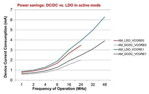
Figure 1: Power saving for an MCU in active mode when using integrated DC/DC vs. LDO
Another way to reduce energy consumption in active mode is to reduce the active duty cycle – the MCU needs to execute the active task as fast as possible before going back to sleep. A Cortex-M4F core can execute a standard MCU task and go back to sleep faster than a Cortex-M0 core, resulting in power savings.
The second optimization an MCU design can make is to leakage current in low-power modes. This is particularly important for higher performance MCUs implemented in smaller process nodes. MCU leakage is affected by two sources: the process technology and the number of gates on or idle in the low-power mode. The first source is geometry-dependent; this is definitely not trivial and can only be done with significant investment and research from MCU vendors to optimize the process technology. Leakage current can also be optimized at the device level. Power gating design techniques can be used to restrict the number of gates powered in sleep mode. Typically only a small number of low-speed peripherals are required to maintain operation and interrupt capability in sleep mode. A robust MCU design can divide up the peripherals into various power domains and completely gate off the power to higher-power and higher-frequency peripherals. On high-performance MCU platforms, active high-performance peripherals are complex and have higher gate counts. Since the low-frequency peripherals are less complex and have less gates, restricting the power to only the essential low-frequency peripherals can significantly reduce leakage current.
Take the power domain concept a step further by dividing power domains into separate high-speed and low-speed peripherals. The transistor technology used for high-speed or low-speed peripherals can also be individualized to yield even further power savings. Figure 2 illustrates an ideal combination of standard voltage threshold (SVT) transistors for high-speed components and high voltage threshold (HVT) transistors for a high-performance, low-power MCU. Memory can also be power-gated. In sleep modes, flash is usually off, while SRAM is in retention-only mode. However, not all SRAM memory needs to be retained as many run-time variables are temporary and need to be recreated after device wake-up.
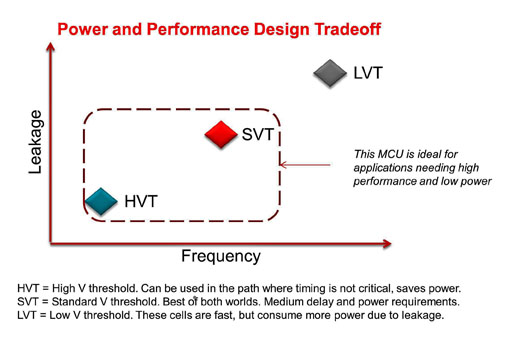
Figure 2: An ideal combination of SVT and HVT transistors on high-performance, low-power MCUs.
Beyond datasheet and power features
Understanding the real-world MCU power efficiency early in the design process is critical. Even small errors in calculating power consumption can lead to significant discrepancies over the application lifetime. Datasheets let developers estimate power consumption, however, innovative power optimization technologies, like those highlighted in this article, make it more difficult to accurately model and profile how an MCU might perform in the field.
To assist developers in evaluating different MCU architectures for power efficiency, the Embedded Microprocessor Benchmark Consortium (EEMBC) has developed the ultra-low-power benchmark standard. ULPBench standardizes datasheet parameters so developers can easily compare power efficiency of different MCUs. It also provides a methodology for measuring MCU energy efficiency in an equitable, reliable and repeatable manner. This methodology includes a variety of tests portable across 8-, 16- and 32-bit MCUs. The benchmark provides a numerical score for each microcontroller’s efficiency. The ULPBench profile can also serve as a reference on how to properly leverage the innovative power features available on an MCU.
Advertisement
Learn more about Texas Instruments


