A recent problem with oscillation in a MOSFET gate driver had an engineer scrambling to find a solution to avoid shutting the production line down. It was hoped that reviewing the board design would uncover clues to the problem and a production-saving solution.
Anyone with experience using high-current, high-speed gate drivers has had their share of challenges with designing a stable circuit. Switching high energy at a MOSFET gate through the driver often causes unwanted oscillation from parasitic inductance in the current path. Two common solutions to address this are:
- Minimize trace inductance, keeping current paths short
- Provide good capacitive bypassing at the supply pins of the gate driver
Sure, it’s common to use bypass capacitors in design, but they are often placed ‘as convenient’ on the circuit board and may not be the ideal values to provide the most impact.
When discussing the transfer of energy, the gate driver can be described as half-bridge switch. It transfers energy from the power source to the gate of the connected MOSFET and the output capacitance of the opposite MOSFET in the output stage. These capacitances are charged through the inductance of the wires, traces, vias, component leads, and die bond wires in the current path. When switching off, the energy in the MOSFET gate returns to the power supply through the low side gate driver switch and through the inductance in the ground path. Each of these two different switching events can lead to troublesome ringing on the supply side and ground side pins of the gate driver.
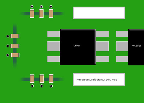
Now consider ways to optimize performance: Storage and bypass capacitors should be placed midway in the current loop that exists between the supply and ground pins of the gate driver (placement along the sides of the gate driver will accomplish this). This breaks up the loop into two approximately equal lengths of parasitic inductance, one from the supply pin of the driver to the positive side of the capacitors, and the other from the ground pin to the negative side of the capacitors. By visualizing the current paths in the layout, the designer can minimize the obstacles placed in the way, including vias, cut outs, mounting holes, and other components. Instead of traces, think of contiguous planes with the mindset of creating wide and short current paths.

Figure 1: Avoid vias and cut outs/voids in the current path
Bypass capacitors decouple and lower the impedance between the supply and the ground pins of the gate driver, thereby effectively shorting out the pins above the rolloff frequency. Consider the frequency response of a capacitor whose impedance approaches zero as frequency increases. The parasitic inductance left in the path creates a notch response as the inductive impedance takes over. This is otherwise known as the self-resonance of a capacitor. The goal becomes to apply more notch responses to broaden the lowered impedance for different ranges of frequencies. A common mistake is to make all the bypass values the same, which simply deepens the impedance notch in a narrow range of frequencies. It is better to use orders of magnitude when selecting bypass values to spread out the notch responses at frequencies ten times above and below.
To be more specific, the engineer introduced earlier in our story experienced approximately 20 MHz oscillations at the output and supply pins of the gate driver. Oscillations also occurred on the negative-going edge, which suggested room for design improvement in the return path on the ground side for discharging the MOSFET gate.

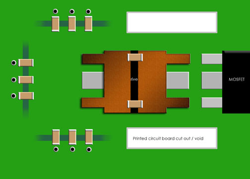
Figure 2: Manually added bypass capacitors and copper tape.
Redesigning a board in production may be impractical, but it may be useful to see what improvements can be made in the future. The gate driver in Figure 2 has two supply and ground pins (left and right, respectively). By soldering copper tape on top of the gate driver, additional bypass capacitance can be added while reducing the parasitic inductance at the same time.
We began with two added capacitors, but found that one 0.01 uF capacitor would eliminate the problem altogether. So, while copper tape soldered on top of the gate driver may not be your final solution, it clearly demonstrates that good placement is critical. The group of four capacitors to the far left have a very long path to the ground pins of the gate driver on the far right. Also, large vias and cutouts that reduce the contiguous planes and narrow the current path are all inductance contributors. Ideal placement would be symmetrically alongside of the gate driver.

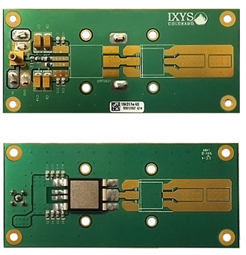
Figure 3: A more optimized layout of bypass capacitors
In terms of specific values, the bypass capacitors used in our engineer’s situation included 100 nF and 470 nF. These values create a deeper notch response to frequency instead of spreading out the individual responses. For example, problems in the tens of megahertz region can benefit from values in the hundreds of nanofarads and then times ten on either side, e.g., 1 uF, 100 nF, and 10 nF.An example of a design with a more optimized layout of bypass capacitors is the DVRFD630 demonstration board in figure 3.
It minimizes loop paths by using contiguous top and bottom ground planes with capacitor placement close to the supply pins of the gate driver. This results in substantially reduced parasitic inductance, and more importantly, oscillation-free performance.
Advertisement
Learn more about IXYS


