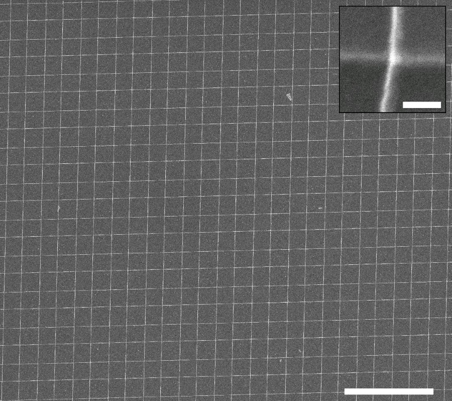
Researchers from Rice University have published a new water-based methodology for manufacturing semiconductors containing patterns of metallic and semiconducting wires less than 10 nanometers wide.  Crossbar array produced with meniscus-mask lithography technique invented at Rice University: crossbar wires are made of silicon dioxide; scale bar is 10 microns and inset scale bar is 100 nanometers.
Referred to as meniscus-mask lithography, the new process holds tremendous promise for a semiconductor industry in dire need of a new way to make circuits even smaller (current integrated circuit fabrication techniques allow for signal wires 10 nanometers wide).
And it’s all possible due to water; well, a physical feature of water. You see, the Rice team figured out that by using the meniscus, the curvy surface of water at its edge, they can create semiconductors with wire patterns between 6 and 16 nanometers wide from silicon, silicon dioxide, gold, chromium, tungsten, titanium, titanium dioxide and aluminum. They have also made crossbar structures of conducting nanowires from one or more of these materials.
Let’s start at the beginning, though: the most common approach to making nanowires is lithography, in which the integrated circuits are etched onto the semiconductor. The problem manufacturers are starting to run into with this approach is that it’s reaching its physical limits — it cannot etch wires smaller than 10 nanometers wide. This is a problem for semiconductor manufacturers, as the industry is dictating technology needs to get smaller.
Bulk synthesis of semiconducting and metallic nanowires less than 10 nanometers wide is a solution, but the wires have so far proven too difficult to position in integrated circuits.
So the researchers turned to water. You see, water tends to adhere to surfaces, and its molecules will gather wherever a raised pattern joins the targeted material, forming a curved meniscus created by the surface tension of the water.
This meniscus-mask, if you will, is what the researchers focused on using. Their methodology proposes adding and removing materials in a sequence that leaves the meniscus covering the wire and climbing the sidewall of a sacrificial metal mask which, when etched away, leaves the nanowires standing alone, and in the exact position it needs to be in.
The method is detailed in the infographic below: Rice lab chemist James Tour, who led the developing of this technique, points out his team’s approach will work with modern fabrication technology with no modifications to existing equipment, and minimal changes in fabrication protocols. Also, there are no new tools or materials needed.
“This could have huge ramifications for chip production since the wires are easily made to sub-10-nanometer sizes,” Tour said of the process. “There's no other way in the world to do this en masse on a surface.”
You can read the full technique in the American Chemical Society journal, Nano Letters.
Via Rice University
Advertisement
Learn more about Electronic Products Magazine


