Heterogeneous computing refers to a growing class of systems in which an application is executed on a mixture of dissimilar processor and accelerator devices to maximize throughput. The execution of a program on this kind of system requires a programming paradigm which presents a consistent system view to the application developer. The OpenCL framework is an industry standard created to address the needs and challenges of heterogeneous compute systems.
At its most fundamental level, the OpenCL framework provides application programmers with a device vendor agnostic definition of a platform and a single memory model across all devices implementing the standard. These characteristics enable an OpenCL programmer to focus on the core challenges of the application being developed and not on the specific details of a particular compute device.
The first component of the OpenCL framework is the platform, which defines the resources available to execute a program. In an OpenCL platform, there is always a host processor and at least one acceleration device. The host processor is responsible for dispatching jobs to the accelerator as well as initiating host/accelerator memory transfers. This host is always implemented using a CPU and the accelerator can be a CPU, GPU, or FPGA. The control of these acceleration devices is through a common set of API functions that are part of the OpenCL standard.
Jobs on an acceleration device take the form of kernel executions. A kernel is the computation function of an application running on an acceleration device. An application in OpenCL may have one or more kernels and each kernel is characterized by expressing a data parallel operation. For example, Figure 1, shows the transformation of a program executing on a CPU to a data and task parallel representation which is suited for OpenCL.
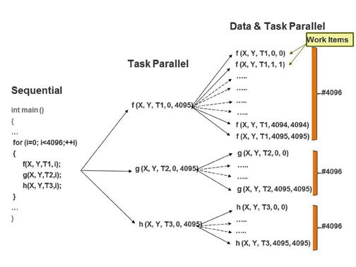
Figure 1: From sequential to a sata and task parallel application
In the sequential version of the code in Figure 1, functions f, g, and h are executed inside of a “for” loop. Each function takes in data sets X and Y as input sources and produces an output T, which is not consumed by any other function inside the “for” loop. Therefore, the loop in the sequential version of the code can be distributed to functions f, g and h to create a task parallel representation of the application as shown by the center column of Figure 1. If each invocation of function f, g and h is independent from both the previous and next invocation then the application is both task and data parallel as shown by the right hand column of Figure 1. Each invocation of function f, g or h represents a work item executed by the acceleration device. Depending on available computation resources, an accelerator can execute all work items in parallel or sequentially.
In addition to presenting the application programmer with a device agnostic data parallel programming model, OpenCL provides a unified memory model hierarchy as shown in Figure 2.
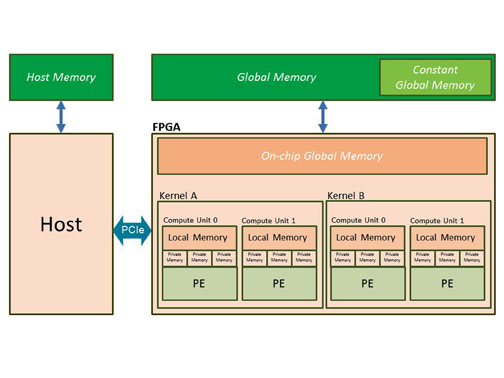
Figure 2: OpenCL memory model
At the application level of the model, the memory space is divided into host memory and device memory. The memory associated with a device is further divided into three levels of hierarchy, including global memory, local memory and private memory. Global memory is created from memory components attached to the device such as SDRAM. The management of buffers mapped onto global memory is handled by the host code application through the usage of OpenCL API functions. OpenCL API functions are used to determine the size of a buffer as well as the read write access to the buffer. Out of all the memory types supported by the OpenCL memory model, it is important to keep in mind that global memory is the memory with the largest capacity and longest latency, thereby defining maximum achievable data throughput and is the only memory that is visible from both the host and the device.
OpenCL and the FPGA
An FPGA can be programmed for different algorithms after fabrication, and, as shown in Figure 3, has look-up tables (LUT) to perform logic operations, flip-flops (FF) to store the result of the LUT, and connections between elements and I/O pads to get data in and out of the IC. Contemporary FPGA architectures incorporate additional computational (DSP), data storage (BRAM), high-speed serial transceivers, and off-chip memory controller blocks. The combination of these elements provides the FPGA with the flexibility to implement custom logic for a given software workload.
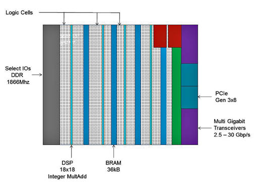
Figure 3: Basic structure of an FPGA
In the context of OpenCL, FPGA fabrics are well suited for this kind of workload due to the data parallel nature of kernel code. Unlike other devices capable of executing OpenCL kernels, the FPGA fabric can be customized with cores that are completely optimized for a specific kernel allowing the parallelism for kernel execution to scale with the size of the FPGA device.
OpenCL applications kernels executed on accelerator compute units. A compute unit refers to the processor core or accelerator logic which executes the operations in the kernel function.
SHA-1 Algorithm
The SHA-1 algorithm is one of the most commonly used cryptographic hash functions. The ability to ensure and check the integrity of data using these kinds of functions has been the basis for online signatures and secure socket layer (SSL) which is at the center of E-commerce solutions. This function is ideally suited for an FPGA since it is composed of and, xor, rotation, add, or and shift operations against a data set of 512 bits through 80 rounds of processing. The 512 bit data load that is used in each round of computation can be computed either in a parallel or block manner.
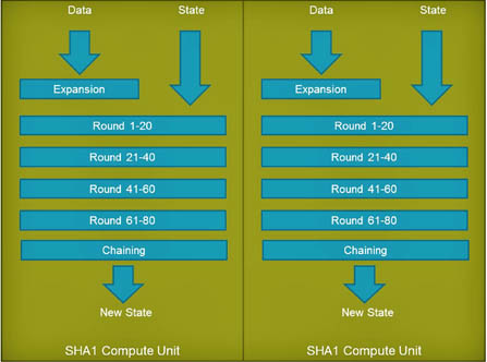
Figure 4: FPGA compute unit for SHA-1
The FPGA implementation of the SHA-1 function is shown in Figure 4. In this design, the key element is the creation of a custom compute unit to encompass the 80 rounds of processing required to compute a single SHA-1. By grouping all 80 rounds of processing inside of the same processing logic, the application designer minimizes interactions with cache or memory elements as would be required in a standard CPU implementation. This in turn increases the throughput for this function and decreases the power consumption needed to sustain the achieved throughput. The advantages of an FPGA implementation vs a CPU implementation are summarized in the following table:
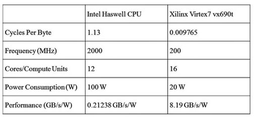
For this comparison, the Intel Haswell CPU has 12 cores capable of executing any OpenCL kernel code but which are not optimized for any specific workload. In contrast, the FPGA implementation has 16 cores optimized to execute only the SHA1 workload. The difference in level of customization for the accelerator compute unit translates directly into the performance difference between the two devices for this workload.
The Xilinx FPGA results were generated by compiling the SHA1 algorithm using the SDAccel development environment for OpenCL, C, and C++ and running the resulting program binary on a Xilinx Virtex 7 device. SDAccel enables up to 25x better performance/watt for data center application acceleration leveraging FPGAs and combines the industry’s first architecturally optimizing compiler supporting any combination of OpenCL, C, and C++ kernels, along with libraries, development boards, and the first complete CPU/GPU-like development and run-time experience for FPGAs.
Advertisement
Learn more about Xilinx


