There are many applications where it is very useful to make analog measurements between separate power domains. Prime examples include industrial feedback systems, motor driver control, and solar inverters. In each case, power buses sitting at fairly high voltage must be monitored and controlled. The device used for controlling these systems typically sits in a much lower power domain (3.3 or 5 V) and all measurements must be isolated.
One way to make an isolated analog measurement is to use a current transfer optocoupler. Consisting of only an LED and a phototransistor, these simple devices enable current applied to the input to be mirrored on the output. They are of limited value for accurate analog measurement and require complex circuitry on the input to condition the signal of interest to drive the LED appropriately. On the output, a buffer is required to use the phototransistor output. Current transfer optocouplers are prone to instability over time and temperature, making it hard to maintain accuracy in critical systems.
Fortunately, there are ways to take advantage of modern isolator technology to make isolated analog measurements. Here are three common ways of taking precision measurements across power domains:
- Use a simple analog circuit and a digital isolator.
- Use a standalone A/D converter for conversion to digital and pair that with a digital isolator.
- Use one of the many analog amplifiers integrated with isolation that are now available.
The analog circuit and isolator combination provides a flexible solution. The analog signal is first amplified to the full-scale input of the second stage — a simple comparator and a ramp oscillator. The signal is converted to a PWM signal and transmitted across a digital isolator. On the opposite side, the signal can be converted back to an analog signal with the appropriate filtering.
The second method replaces the discrete circuit with an A/D. Although this might seem simpler than converting the signal to PWM, it introduces other complications and may actually be more complex. In most cases an amplifier will again be needed as a first stage. Most likely a clock signal, along with other control signals, must be provided to the A/D. These signals can be provided by a dedicated MCU on the opposite side of the isolation barrier but will require the use of multiple channel isolators with channels going each direction. Once the signal is passed across the isolation barrier, conversion back to analog is similarly complex, requiring some type of controller and a D/A converter.
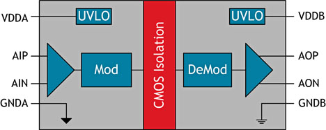
The third method is the most direct. Many CMOS-based products are available today that combine an analog amplifier with an isolation device. The isolated amplifier devices often have inputs scaled for the most common measurement – current via a shunt resistor. No additional circuitry is needed. The signal source is connected directly to the device, galvanic isolation is supported internally, and a reproduced analog signal is provided at the output. The chips isolation technology is key to reduced variation with temperature and age, tighter part-to-part matching, and longer lifetimes compared to other isolation technologies.

Fig. 1: A block diagram of a galvanically isolated analog amplifier.
You can find a reasonably priced standalone analog isolator amplifier that uses the latest isolation technology. The isolation barrier is robust while the signal remains stable and accurate. The integrated circuits input has the attributes of low offset and gain drift, low noise, and high linearity to ensure precise measurement.
One example of many available galvanically isolated analog amplifiers is the Si8920 from Silicon Labs. The device's low voltage differential input is ideal for measuring voltage across a current shunt resistor. Its output is a differential analog signal amplified by either 8.1x or 16.2x.
The IC's very low signal delay of 0.75 µs allows control systems to respond quickly to fault conditions or changes in load. Low 1 µV/°C offset drift and 60 ppm/°C gain drift ensure that accuracy is maintained over the entire -40° to 125°C operating temperature range and gain error is less than 0.5%. Noise is specified as 0.10 mVrms over a 100 kHz bandwidth. and nonlinearity is 0.1% full-scale.
The device's high 75 kV/µs common mode transient immunity means it can deliver accurate measurements even in the presence of high power switching like would be found in a motor drive system or inverter. It supports up to 5.0 kVrms withstand voltage per UL1577.
Advertisement
Learn more about Silicon Labs


