Many industrial and medical applications use instrumentation amplifiers (INA) to condition small signals in the presence of large common-mode voltages and DC potentials. The three-op-amp INA architecture performs this function with the input stage providing a high input impedance, while the output stage filters out the common-mode voltage and delivers a differential output. High impedance coupled with high common-mode rejection is the key to many sensor and biometric applications including flow sensors, temperature sensors, weigh scales, electrocardiogram (ECG), and blood glucose meters. We will look at the three-op-amp INA and examine the advantages of zero-drift amplifiers, RFI input filters, and programmable gain amplifiers. We’ll also look at an application for a sensor health monitor.
The three-op-amp INA
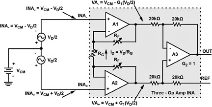
By their very nature, INAs are a good choice to condition small signals. Their high-input impedance is achieved by using the non-inverting inputs of the input stage, without having to resort to any feedback tricks (see Figure 1). The three-op-amp circuit strips off the common-mode voltage and amplifies the sensor signal with very little error. However, the input common-mode voltage and the differential voltages must be taken into account to avoid saturating the INA’s input stage. A saturated input stage may appear normal to processing circuitry, yet have disastrous consequences. Providing maximum design margin by using amplifiers with rail-to-rail input and output configurations will help avoid this input saturation.

Fig. 1: Block diagram of three-op-amp INA with voltage nodes.
The input offset voltage of all amplifiers, regardless of process technology and architecture, will vary over temperature and time. Manufactures specify input offset drift over temperature in terms of V/°C. Traditional amplifiers will spec this limit at several microvolts to tens of microvolts. This offset drift can be problematic in high-precision applications and cannot be calibrated out during initial manufacturing. An amplifier’s input offset voltage can also drift over time and can create significant errors over the life of the product. This drift is usually not specified in datasheets.
Zero-drift devices
Zero-drift amplifiers continually self-correct the offset voltage. Some devices correct the offset as often as 10,000 times a second. Zero-drift amplifiers can deliver offset drift as low as 5nV/°C. Zero-drift amplifiers can also eliminate 1/f noise, or flicker noise (see Figure 2). 1/f noise is a low-frequency phenomenon caused by irregularities in the conduction path and noise due to the currents within the transistors. This makes zero-drift amplifiers ideal for low-frequency input signals such as outputs from strain gauges, pressure sensors, and thermocouples.
A designer should consider that the zero-drift amplifier’s sample-and-hold function turns it into a sampled-data system, making it prone to aliasing and fold-back effects due to subtraction errors, which cause the wideband components to fold back into the baseband. However, at low frequencies, noise changes slowly, so the subtraction of the two consecutive noise samples results in true cancellation.

Fig. 2: Noise density in semiconductors: 1/f noise to white noise.
The need for an input filter
The proliferation of wireless transceivers in portable applications has led to increased attention to a circuit’s ability to operate near radio transmitters. As a result, RF suppression is needed to ensure interference-free operation of the sensor/amplifier.
The high-frequency RF signal can appear as a rectified DC offset at the output of precision amplifiers. Because the gain of the precision front end can be 100 or greater, it is critical not to amplify any conducted or radiated noise that may be present at the amplifier inputs. An easy solution to this problem is to include RFI filters on the inputs of the INA.
It is widely accepted that you cannot build a precision differential amplifier using discrete parts and obtain good CMR performance or gain accuracy. This is due to the matching of the four external resistors used to configure the op amp into a differential amplifier. While integrated solutions improve on-chip resistor matching, there remains a problem with absolute matching to the external resistors used to set amplifier gain. This is because of the combined tolerance of on-chip and external precision resistors. Another source of error is the difference in thermal performance. It is possible for the internal and external resistors to have opposite temperature coefficients. A programmable gain amplifier solves this problem by having all the resistors on board. The gain error for this type of amplifier can be less than 1%, with typical trim capabilities of the order of ±0.05%; and ±0.4% maximum across temperature.
Easy sensor health monitoring
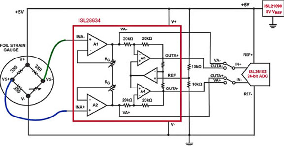
A bridge-type sensor uses four matched resistive elements to create a balanced differential circuit. The bridge can be a combination of discrete resistors and resistive sensors for quarter-, half-, and full-bridge applications. The bridge is driven by a low-noise, high-accuracy voltage reference on two legs. The other two legs are the differential output signal. In a bridge circuit, the differential signal’s common-mode voltage is the “midpoint” potential voltage of the bridge excitation supply, or +2.5 V in a single supply +5 V system.

Fig. 3: Sensor health monitor application schematic.
The concept of sensor health monitoring is to keep track of the bridge impedance within the data-acquisition system. Changes in the environment, degradation over time, or a faulty bridge-resistive element will imbalance the bridge and cause errors. You can measure the bridge differential output common-mode voltage to determine the sensor’s impedance health (see Figure 3).
There are many instrumentation amplifiers available from many manufacturers. One excellent example would be the ISL28633 rail-rail I/O, zero-drift, programmable gain device from Intersil. This TSSO14 packaged amp runs on 5 V, has a CMRR of 138 dB and a gain of 100, gain error of less than 0.4% maximum, and input offset voltage of 5 µV maximum.
Advertisement
Learn more about Intersil


