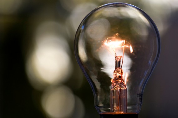
Traditional, incandescent light bulbs have long been on their way out.

First made commercially available by Thomas Edison, the technology has remained largely unchanged for more than a century now: it still works by heating a thin tungsten wire to extremely hot temperatures (approximately 2,700 degrees Celsius) which, in turn, causes the wire to emit what’s referred to as black body radiation, or a broad spectrum of light.
The problem with this source of light is efficiency: more than 95% of the bulb’s energy is wasted, a vast majority of which is spent in the form of heat. This has led to many countries banning the bulb, or otherwise phasing it out, in favor of more efficient compact fluorescent lightbulbs (CFLs) and light-emitting diode (LED) blubs.
But researchers at MIT and Purdue University believe they’ve found a second life solution for incandescent light bulbs via a newly developed two-stage process. The first stage uses a conventional heated metal filament, unchanged so as to allow it to expel all of its expected losses; however, rather than allow for the waste heat to dissipate as infrared radiation, secondary structures surround the filament to capture said radiation, and reflect it back to the filament to be re-absorbed and re-emitted as visible light.
These structures are a form of photonic crystal, consisting largely of Earth-abundant elements, and can be made using conventional material-deposition technology.
The second stage improves upon the efficiency with which incandescent light bulbs convert electricity into light. The reason why this is being addressed is because at present, current incandescent bulbs fall into a range of about 2 to 3% when it comes to efficiency. For comparison purposes, CFLs fall between 7 and 13%, while LEDs are between 5 and 13%. The team reports their new approach could reach efficiencies as high as 40%. In terms of what they’ve achieved thus far, the first proof-of-concept bulb has achieved about 6.6% efficiency.
The success of this update is due in large part to the team’s designing of a photonic crystal that is able to work for a very wide range of wavelengths and angles. The crystal itself is made of thin layers, all of which are deposited on a substrate. By figuring out the right thickness and sequence of these layers, the team was able to tune how the materials interact with the light. Specific to their system, the desired visible wavelengths travel right through the material and on out of the bulb, but the infrared wavelengths are stopped by and reflected off the bulb as though it were a mirror. They then travel back to the filament, adding more heat which, in turn, gets converted to more light. And since it’s only visible light that escapes the bulb, the heat just keeps bouncing back in toward the filament until it finally ends up as visible light.
The potential of this technology looks to be far reaching. Beyond bulbs, the idea of reflecting heat could significantly improve the performance of energy-conversion schemes like thermo-photovoltaics, wherein heat from an external source helps make a material glow, thereby causing it to emit light which can then converted into electricity by a photovoltaic absorber.
Read the full study, entitled “Tailoring high-temperature radiation and the resurrection of the incandescent source”, which was published in the journal Nature Nanotechnology.
Via MIT
Advertisement
Learn more about Electronic Products Magazine


