By KEVIN TOMPSETT
Senior Applications Engineer
Analog Devices
www.analog.com
These days switching power supplies are nearly ubiquitous and used throughout every electronic devices. They are valued for their small size, low cost, and efficiency. However, they have the major drawback in that their outputs can be noisy due to the high switching transients. This has kept them out of high performance analog circuits where linear regulators have ruled the roost. It has been shown that in many applications an appropriately filtered switching converter can replace a linear regulator for production of a low noise supply. Even in those demanding applications where an extremely low noise supply is required, there is probably a switching circuits somewhere upstream in the power tree anyway. Therefore there is a need to be able to design optimized, dampened multistage filters to clean up the output from switching power converters. In addition it is important to realize how the filter design will affect the compensation of the switching power converter.
In this article, boost circuits will be used for the example circuits, but the results will be directly applicable to any dc/dc converter. Shown in Fig. 1 are the basic waveforms in a boost converter in constant-current mode (CCM).
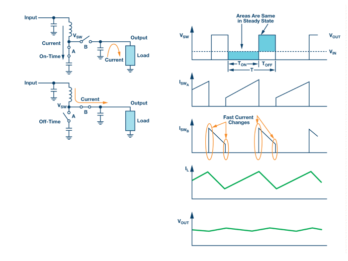
Fig.1: Basic voltage and current waveforms for a boost converter
The issue that makes an output filter so important for a boost or any of the other topologies with discontinuous current mode (DCM), is the fast rise and fall in the current time in switch B. This tends to excite parasitic inductances in the switch, the layout, and the output capacitors. The result is that in the real world the output waveforms look much more like Fig. 2 rather than Fig. 1 even with good layout and ceramic output capacitors.
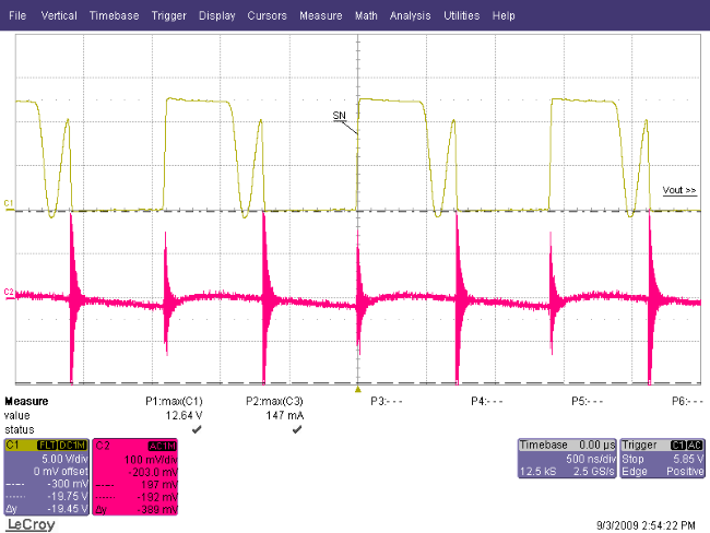
Fig.2: Typical measured waveforms of a boost converter in DCM
The switching ripple (at the switching frequency) caused by the change in charge of the capacitor is very small compared to the undampened ringing of the output switch which we will refer to as output noise. Generally, this output noise is in the 10-100+ MHz range, well beyond the self-resonant frequency of most ceramic output capacitors. Therefore adding additional capacitors will do little to attenuate the noise.
There are a couple of reasonable choices for different types of filters to filter this output. This article will illustrate each type of filter and give a step by step process to a design. The equations are not rigorous and some reasonable assumptions are made to simplify them somewhat. There is still some iteration required since each component will affect the values of the others. The ADIsimPower design tools get around this problem by using linearized equations for component values, like cost or size, to do an optimization before actual components are selected, and it then optimizes the outputs once real components are chosen from the database of thousands of parts. However, for a first pass at a design, this level of complexity is not necessary. With the provided calculations and possibly using a SIMPLIS simulator like the free ADIsimPE, or some bench time in the lab, a satisfactory design can be found with a minimal amount of effort.
One thing to consider before designing the filter is consider what is achievable with a single stage filter RC or LC filter. Typically with a second stage filter it is reasonable to get the ripple down to a few hundred µV pp and the switching noise down below 1 mV pp. A buck converter can be made somewhat quieter since the power inductor provides significant filtering. These limitations are because once the ripple is down in the uV the component parasitics, and noise coupling between filter stages starts to become the limiting factors. If even quieter supplies are required, then a third stage filter can be added. However switching power supplies do not generally have the quietest references and also suffer from jitter noise. These both result in low frequency noise (1 Hz-100 kHz) which cannot be easily filtered out. Therefore for extremely low noise supplies it may be better to use a single second stage filter and then add an LDO to the output.
Before diving into a more detailed design process for each type of filter, some values which will get used in the design process for each of the types of filters are defined below.
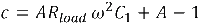
ΔIpp is the approximate peak to peak current coming into the output filter. For the calculations we assume that this sinusoidal. The value will depend on the topology. For a buck it is the peak to peak current in the inductor. For a boost converter it is the peak current in switch B (often a diode).

is the approximate out voltage ripple at the switching frequency of the converter
RESR : is the ESR of the chosen output capacitor.
FSW : Switching frequency of the converter
Crip : The output capacitor calculated assuming all of ΔIpp rip flows into it

The change in Vout when Istep is applied to the output
Istep : An instantaneous change of the output load.
Tstep : The approximate response time of the converter to an instantaneous change in the output load
Fu : The crossover frequency of the converter. For a buck it is generally FSW /10. For a boost or buckboost type converter it is generally about a third of the location of the right half plane zero (RHPZ).
The simplest type of filter is just an RC filter as shown attached to the output of a low current ADP161x based boost design shown in Fig. 3 . This filter has the advantage of low cost and will not need to be damped. However, due to power dissipation it is only useful for very low output current converters. For this article ceramic capacitors with small ESR are assumed.
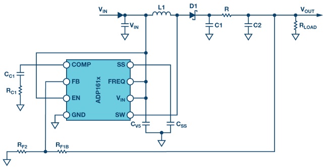
Fig. 3: ADP161x low output current boost converter design with an added RC filter on the output.
Design process for an RC second stage output filter:
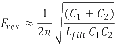
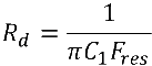
Step1 : choose C1 based on assuming the value output ripple at C1 is approximately ignoring the rest of the filter 5-20 mV pp is a good place to start. C1 can then be calculated using equation 1.
1.
Step2 : R can be chosen based on power dissipation. R must be much larger than RESR for the capacitors, for this filter to be effective. This limits the range of output currents to something less that 50 mA or so.
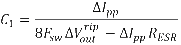
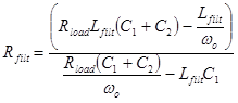
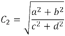
Step3 : C2 can then be calculated from equation 2 through equation 6. A,a,b,and c are just intermediate values to simplify calculation and have no physical meaning. These equations assumes Rload and the ESR for each capacitor is small. These are both very good assumptions and introduce little error. C2 should be the same or larger than C1. The ripple in step 1 can be adjusted to make this possible.
2.

3.

4.

5.
6.
For higher current supplies it is beneficial to replace the resistor in the pi filter with an inductor as shown in Fig. 4 . This configuration gives very good ripple and switching noise rejection in addition to low power loss. The issue is that we have now introduced an additional tank circuit that can resonate. This can result in oscillations and an unstable power supply. Therefore the first step to designing this filter is to figure out choose how to damp the filter. Figure 4 shows three viable damping options. Adding Rfilt has the advantage of adding little extra expense, or size. The dampening resistor typically has little to no loss and can be small for even large power supplies. The drawback is that it significantly reduces the effectiveness of the filter by reducing the parallel impedance with the inductor. Option two has the advantage of maximizing filter performance. If an all ceramic design is desired Rd can be a discreet resistor in series with a ceramic capacitor. Otherwise a physically large capacitor with a high ESR is required. This additional capacitance (Cd) can add significant cost and size to the design. Damping option three looks very advantageous since the dampening capacitor Ce is added to the output where it might help somewhat with transient response and output ripple. However, this is the most expensive option since the amount of capacitance required is much larger. In addition, the relatively large amount of capacitance on the output will lower the frequency of the filter resonance which will reduce the achievable bandwidth of the converter, therefore technique 3 is not recommended. For the ADIsimPower design tools we use technique 1 because of the low cost and relative ease of implementing it in an automated design process.
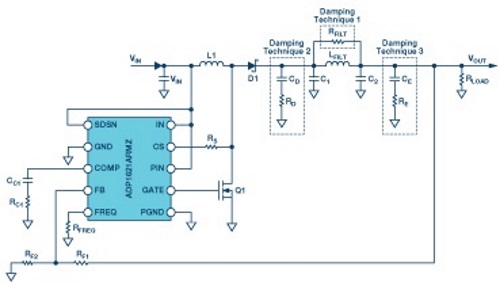
Fig. 4: AN ADP1621 with an output filter with several different dampening techniques highlighted
Another issue that needs to be dealt with is compensation. It may be counterintuitive, but it is almost always better to put the filter inside the feedback loop. This is because putting it in the feedback loop helps damp the filter somewhat, eliminates dc load shift, the series resistance of the filter, and gives better transient response with less ringing. Figure 5 shows the Bode plot for a boost converter with an LC filter output added to the output.
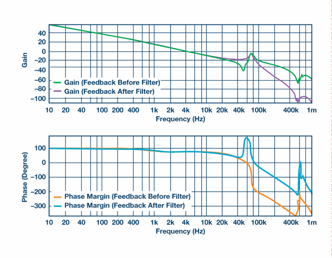
Fig. 5: Phase and gain plots for a boost converter with an LC filter on the output.
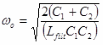
The feedback is taken before or after the filter inductor. The thing that is most surprising to people is how much the open loop Bode plot changes even when the filter is not “in” the feedback loop. Since the control loop is affected with or without the filter in the feedback loop, one might as well compensate for it appropriately. In general this will mean scaling back the target crossover frequency to a maximum of a fifth to a tenth of the filter resonant frequency (Fres ).
7.
The design process for this type of filter is iterative in nature since each component selection drives the selection of the others.
Design process for an LC filter using a parallel resistor damping (technique 1 in Fig. 4)
Step1 : Choose C1 as if there was not going to be an output filter on the output. 5-20 mVpp is a good place to start. C1 can then be calculated using equation 8.
8.
Step2 : Select the inductor Lfilt. Based on experience, a good value is between 0.5 μF to 2.2 μF. The inductor should be chosen for a high self-resonant frequency (SRF). Larger inductors have larger SRFs which means they are less effective for high frequency noise filtering. Smaller inductors will not have as much effect on ripple and will require more capacitance. The higher the switching frequency is the smaller the inductor can be. When comparing two inductors with the same inductance, the part with higher SRF will have lower inter-winding capacitance. The inter-winding capacitances acts like a short circuit around the filter for high frequency noise.
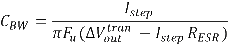
Step3 : As described above, adding the filter will affect the compensation of the converter by reducing the achievable crossover frequency (Fμ) . For a current mode conversion the maximum achievable is the lesser of 1/10 of the switch frequency, or 1/5 the FRES of the filter as calculated in equation 7. Fortunately, most analog loads do not require exceptionally high transient response. Equation 9 calculates the approximate output capacitance (CBW ) required on the output of a converter to provide for a specified transient current step.
9.
Step4 : Set C2 as the minimum of CBW and C1
Step5 : Calculate the approximate damping filter resistance using equations 10 and 11. These equations are not absolutely accurate, but they are the closest thing to a closed form solution without the need to use extensive algebra. The ADIsimpower design tools calculate Rfilt by calculating the open loop transfer function (OLTF) of the converter with the filter and with the inductor shorted out. Rfilt values are then guessed until the peak of the converter OLTF with the filter is only 10 dB above the OLTF of the converter with the inductor shorted. This technique can be used in a simulator like ADIsimPE or in the lab using a spectrum analyzer.
10.
11.
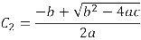
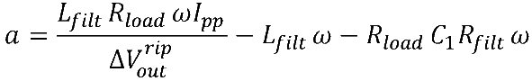
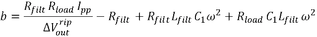
Step5 : can now be calculated using equations 12 -15. a, b, c, and d are used to simplify equation 16.
12.
13.
14.

15.

16.
Step6 : Step 3 through 5 should be repeated until a well-damped filter design is calculated that meets the required ripple and transient specifications. It should be noted that these equations ignore the DC series resistance of the filter inductor RDCR . This resistance can be quite significant for lower current supplies. It improves filter performance by helping to dampen the filter which increases the required Rfilt and increasing the impedance of the filter. Both effects can significantly improve the performance of the filter. It can therefore be very helpful for low noise requirements to trade off a small amount of power loss in Lfilt for improved noise performance. Core loss in Lfilt also helps to attenuate some of the high frequency noise therefore the high current-powdered iron core can be a good choice. They also tend to be smaller and cheaper for the same current capability. ADIsimpower of course factors in both the resistance of the filter inductor in addition to the ESR of the two capacitors for maximum accuracy.
Step7 : When choosing actual components to match the calculated values, remember to derate the capacitances of any ceramic capacitors to account for DC bias!
As stated previously Fig. 4 gives two viable options for damping the filter. If instead of choosing a parallel resistor, a capacitor can be chosen to damp the filter. This will add some cost, but it provides the best filter performance of any option.
Design process for an LC filter using an RC damping network (technique 2 in figure 4)
Step1 : As in the previous topology, choose C1 as if there were not going to be an output filter. 10-100 mVpp is a good place to start, depending on the final target output ripple. C1 can then be calculated using equation 8. C1 can be smaller in this topology than the previous topologies because the filter is more effective.
- Step2 : As in the previous topology an inductor between 0.5-2.2 H is chosen. 1 mH is a good value for converters between 500 and 1,200 kHz.
- Step3 : As before C2 can be chosen from equation 16, but with Rfilt set to something large like 1 MΩ since it will not be populated. The reason this is the same value even though I am adding an additional capacitor to C1 is that in order to provide good damping, Rd will be made large enough that Cd will not significantly reduce the ripple. Set C2 as the minimum of the calculated C2 value, CBW and . It can be useful at this point to return to step 1 and adjust the ripple assumed on C1 to get a calculated C2 that is closer to CBW and C1 .
Step4 : Cd should be set to the same value as C1 . In theory you can achieve more damping of the filter using a larger capacitance, but it needlessly adds cost, size, and can reduce converter bandwidth.
Step5 : Rd can be calculated from equation 17. Fres is calculated using equation 7, ignoring the presence of Cd . This is a good approximation since Rd is typically large enough that Cd will have little effect on the location of the filter resonance.
17.
Step6 : Now that both Cd and Rd have been calculated either a ceramic capacitor with a series resistance can be used, or a tantalum or similar capacitor with large ESR should be chosen that matches the calculated specifications.
Step7 : When choosing actual components to match the calculated values, remember to derate the capacitances of any ceramic capacitors to account for dc bias!!
Another filter option is to replace the L in the previous filter with a ferrite bead. However, this arrangement has a lot of drawbacks that limit its effectiveness at filtering switching noise and does almost nothing for switching ripple. First is saturation. The ferrite bead will saturate at a very low level of bias current, meaning that the ferrite will give much lower impedance than shown in the zero bias curves shown in all datasheets. It may still need damping since it is still an inductor and therefore can resonate with the output capacitance. However, now the inductance is variable and poorly characterized in the very minimal data provided in most datasheets. For this reason ferrite beads are not recommended for use as a second stage filter, but can be used downstream from one to further reduce very high frequency noise.
This article laid out several output filter options for switching power supplies. For each topology, a step by step design process has been devised to reduce the amount of guess and check required for filter design. The equations have been simplified somewhat so that they are useful to an engineer looking to do a quick design by understanding what is achievable from a second stage output filter.
Advertisement
Learn more about Analog Devices, Inc.


