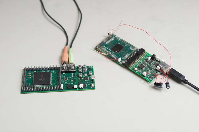
While the analog vs digital chip has been trending towards the latter in recent years, a breakthrough by researchers from the Georgia Institute of Technology might shift things the other way.
The team there has successfully built and demonstrated a configurable analog chip that not only can compute using 1,000 times less electrical power than comparable digital floating-gate configurable devices already in use, it can also be scaled down to a hundred times smaller.

The new device, referred to as the Field-Programmable Analog Array (FPAA) System-On-Chip (SoC), uses analog technology supported by digital components to achieve this never-before-seen level of power and size reduction capability.
At present, field programmable gate arrays (FPGAs) are the preferred device in the configurable chip market. One of the main reasons why is because they can be altered internally at any given moment, and techniques to reconfigure them for several different forms and functions are already well-established.
Researchers took these key advantages into consideration when developing the FPAA device, establishing a programming interface remarkably similar to the digital circuits.
“But in other ways the FPAA is going to seem quite different,” said Jennifer Hasler, a professor in the Georgia Tech School of Electrical and Computer Engineering (ECE) and leader of the research team that produced the new analog architecture
“In terms of the power needed, it's extremely different because you need only milliwatts to run the analog device, while it's hard to get an FPGA to work on less than a watt.”
A broad stroke listing of the advantages:
• The FPAA device is non-volatile, meaning it retains data even when power is turned off (similar to flash memory technology) and it use less power than volatile SRAM configurations (like those used in FPGAs).
• The unique analog architecture of these FPAAs allows for computing via the routing fabric of the chip, thereby exploiting areas usually considered useless. Specifically, this was made capable by way of highly efficient switches that can be programmed on, off, or in-between – partially on and partially off. Such flexibility provides increased computation capabilities as well as reduced power consumption.
• The FPAA device operates on less than 30 milliwatts, literally thousandths of a watt, which is nearly three orders of magnitude less than a conventional digital configurable chip. The researchers believe further design advances in analog arrays could bring their power needs down into the microwatt range, or millionths of a watt.
Now, two things worth taking a closer look at about the FPAA technology:
First, to program the analog environment of the device, electrons are manipulated in a very precise way using electron-injection and electron-tunneling techniques. This approach allows for the erasing of data by lowering the number of electrons at specific locations in the device structure to the lowest possible value.
New data, on the other hand, is encoded by increasing the number of electrons located at a given location up to an exact value.
It sounds incredibly complex, but this solution allows for a highly dense chip structure which, in turn, makes it possible for several programmable variables to exist in a large number of different states.
“Our FPAA chip has roughly half a million of these programmable parameters,” Hasler explains. “They can be used as a switch in a digital manner – using the lowest possible value for 'off' or the highest possible value for 'on' – or we can achieve even more rich behavior using intermediate values.”
The other thing about the FPAA worth pointing it out is that it includes a small amount of built-in digital circuitry for the purpose of supporting communication within the chip and to also help run the programming infrastructure. These support features provide engineers with an extensive set of helpful, high-level programming tools (example: working with analog arrays is now accessible to those familiar with digital designs, which are programmed using similar high-level tools as that which is found in the FPAA). The toolset can both simulate and program the FPAA reconfigurable device.
“Our toolset uses high-level software developed in the Scilab/Xcos open-source programs, with an analog and mixed-signal library of components,” Hasler said. “Georgia Tech undergraduates are already using these tools in classes in the School of Electrical and Computer Engineering that cover mixed-signal and analog devices and tools.”
Looking ahead, Hasler said that she and her team have spoken with numerous companies about potential applications, including businesses in the commercial, military, and neuromorphic sectors, among others. A number of FPAA chips have already been produced, but plans for scaling up the manufacturing of this device has not been finalized yet.
Also, the key technologies in the FPAA SoC are patent pending.
Learn more by downloading any of the published materials below:
Integrated Floating-Gate Programming Environment for System-Level ICs
A Programmable and Configurable Mixed-Mode FPAA SoC
An Open-Source Tool Set Enabling Analog-Digital-Software Co-Design
Via the Georgia Institute of Technology
Advertisement
Learn more about Electronic Products Magazine


