Diamonds have long been looked at as a potential source for semiconductors. The reasons are plentiful, but chief among them are the diamond’s superior thermal properties, especially when compared to those of silicon.

The problem with using diamonds as semiconductors lies in doping diamond-based devices. This is an extremely difficult process, especially for n-type semiconductors.
Researchers from the University of Wisconsin (Madison) and the University of Texas (Arlington) believe they’ve taken a first step to resolving this issue. They recently published a report that describes a new doping method they believe could help the diamond realize its full potential as a semiconductor.
In order to better understand this new technique, it is important to first understand modern methods. At present, diamond-doping techniques call for coating the crystal with boron and heating it to 1450 degrees Celsius. It’s a good technique, up until the diamond has cooled, at which point the boron coated to the diamond needs to be removed; something that is very difficult to do.
Additionally, while this method works nicely for diamonds made up of multiple crystals stuck together, poly-diamonds structures are fraught with irregularities at the points where the crystals structures meet, making them a less desirable solution compared to single-crystal diamonds.
And if you want to use single-crystal diamonds, you must first inject boron atoms into the crystals as they’re grown. To do this, you need a microwave, and a powerful one at that. In fact, the microwave needs to be so powerful (to inject the boron atoms), it actually degrades the diamond crystal when the material is run through it.
What the team figured out is that if they bonded a single-crystal diamond with a piece of silicon doped with boron, they need only heat it to 800 degrees Celsius in order to get the boron atoms to migrate from the silicon and attach to the diamond.
The way it works is the atoms migrate during the heating process, creating vacancies filled by the boron. Specifically, carbon atoms from the diamond shift to fill defects such as atom vacancies within the lattice structure. As they move, vacancies are left in the diamond’s structure; these are, in turn, filled by the boron atoms.
Worth pointing out is the fact that this new method allows for selective doping; this, in turn, allows for greater control when making diamond semiconductor-based devices. It is achieved by bonding the silicon to a specific spot on the diamond crystal.
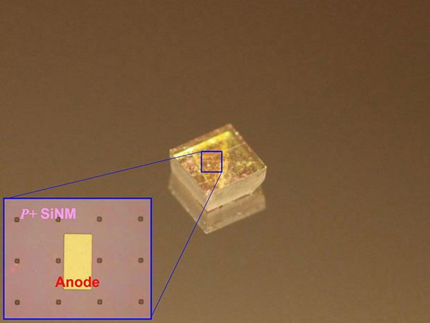 Diode array on a natural single crystalline diamond plate; inset shows deposited anode metal atop heavy-doped silicon nanomembrane bonded to natural single crystalline diamond.
Now, it should be noted that the team’s solution addresses issues tied to p-type doping only — it gives diamonds positive charge carriers. It doesn’t address n-type doping, which remains a more problematic process. To truly consider this study a success, the Wisconsin-Texas team will need to figure out a way to take this next step.
In the meantime, they will work on creating a simple device using p-type single-crystal diamond structures.
“We feel like we found a very easy, inexpensive, and effective way to do it,” said Zhengqiang (Jack) Ma, one of the authors of the research. He added that achieving p-type doping is an important success, and that he is hopeful other teams will find solutions for creating n-type single-crystal diamonds.
Via IEEE
Advertisement
Learn more about Electronic Products Magazine


