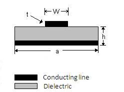
Microstrip transmission lines are widely used, providing compact and lightweight electronic circuits that are readily adaptable to hybrid and monolithic integrated-circuit (IC) fabrication technology. Understanding the fundamentals of microstrip transmission lines is an imperative step in leveraging the technology to meet your design goals, so let’s review:
The microstrip line is a type of electrical transmission line that can be fabricated through printed circuit boards, and used to carry Electro-Magnetic Waves (EM waves) or microwave frequency signals. It consists of a single conductor strip on one side of dialectic or insulating substrate and a single ground plate on the opposite side. Since the conductor strip side is exposed to air, these transmission lines can only exist on top and bottom (PCB) layers. The structure can be built in materials other than printed circuit boards, but will always consist of a conductor separated from a ground plane by some dielectric material. Its effective resistance is influenced by both the dielectric of the substrate material and the air above it. Since it is an open structure, microstrip line has a major manufacturing advantage, and is used to design and fabricate RF and microwave components such as antennas , couplers and power divider/combiners, among others
Products made using microstrip lines exist as a pattern of metallization on the substrate, making them less expensive and lighter in weight compare to traditional waveguide technology. FR-4 dielectric substrate (laminated by a thin layer of copper foil) is usually used as PCB for microstrip-based etching due to its low cost, as they are simple to produce, and operate over a wide bandwidth, within small weight and dimensions. Microstrip lines have low to high radiation, support 20 to 120 ohm impedance as well as quality (Q) factors of about 250, corresponding to a narrower bandwidth.
Microstrip transmission lines suffer from three types of losses: conductor, dielectric, and radiation losses. Conductor loss is dependent on the type of metal used for the transmission lines and the dimensions of those lines, with loss increasing with length.
Dielectric loss is a function of the type of PCB substrate material, although you can (approximately) cut metal losses in half by doubling the dielectric thickness and keeping the same system. Lastly, since all active components must exist on the top and bottom PCB layers, the microstrip is not enclosed, allowing the circuits to potentially radiate, causing unintended circuit response.
The microstrip is simple to produce, operates over a wide bandwidth, and has small weight and dimensions, making it a comparable transmission line to traditional waveguide technology.
Sources: BitWeenie, Microwave Journal, Microwaves 101, EEWeb
Advertisement
Learn more about Electronic Products Digital


