Dialog Semiconductor is demonstrating the DA8801, its first GaN power IC product, using TSMC's 650-V GaN-on-Si process technology. The DA8801, together with the company’s patented digital Rapid Charge power conversion controllers, enable more efficient, smaller, and higher-power density adapters compared to traditional silicon FET-based designs. It is initially targeting the fast-charging smartphone and computing adapter segment with its GaN solutions.
See SmartGaN video from Dialog Semiconductor.
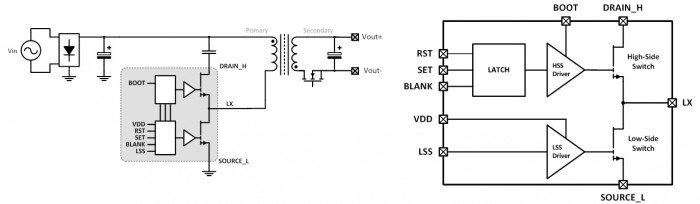
The entry by Dialog into the wide band-gap technology is significant because it’s a consumer product as opposed to high-end commercial products used by server farms or telecom companies. It means that GaN designs are now competitive with Si-based consumer designs. These GaN-based designs deliver much better efficiency in a smaller area. GaN technology offers the world’s fastest transistors, which are the core of high-frequency and ultra-efficient power conversion. Dialog’s DA8801 half-bridge integrates building blocks, such as gate drives and level-shifting circuits, with 650-V power switches to deliver a solution that reduces power losses by up to 50%, with up to 94% power efficiency. It allows a reduction in the size of power electronics by up to 50%, enabling a typical 45-W adapter design today to fit into a 25-W form factor. This reduction in size will enable true universal chargers for mobile devices. The product allows for a seamless implementation of GaN, avoiding complex circuitry, needed to drive discrete GaN power switches. The DA8801 will be available in sample quantities in Q4 2016. Find more information at: http://www.dialog-semiconductor.com/products/DA8801.
Advertisement
Learn more about Dialog Semiconductor


