By ALI FAWAZ
Senior Staff Application Engineer,
Infineon Technologies,
www.infineon.com
Developing a switched-mode power supply for dimmable LED fixtures is a significant engineering effort. Changes in the specification of the actual lighting elements or the functionality of the fixture, such as different current supply, modulation levels or minimum dimming levels, can trigger a cascade of changes in the various components or even a complete redesign. So it’s not surprising that lighting engineers are working both to reduce the component count and increase the flexibility of a completed design.
While we’ve seen a great deal of innovation in areas such as digital controllers, the interface between the physical dimming control and driver ICs remains complex. Typically, a potentiometer or 0-10V dimmer is the source of an initial voltage input. An interface to the driver IC is used to produce a digital PWM signal used by controller IC. This is implemented with either a transformer or optocoupler-based circuit, as seen in Fig. 1 . Each of the components (from 10 – 30 depending on the design) adds to the evaluation, test, and of course, assembly costs for the fixture.
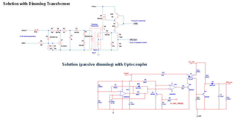
Fig. 1: Typical LED dimming interface circuit designs
Integration of these discrete functions in an IC suitable for an LED power supply is challenging because of frequently changing design parameters. For example, dimming systems used to control multiple luminaires require a different bias current setting than a short string. Duty cycle variations that are traditionally managed by changes in the transformer design can be managed by an IC. A transformer can add 30-50 cents to system cost and needs a large amount of board real estate, so a solution that eliminates the component is desirable.
A suitable IC that accommodates variable requirements while minimizing design complexity and component count is the recently introduced CoolDIM10V dimming interface. The IC converts an analog voltage signal from a 0-10 V dimmer or potentiometer to a current-based PWM signal. The dimming signal is routed through an external optocoupler to achieve galvanic isolation as the signal is passed to the lighting controller IC, as seen in Fig. 2 .
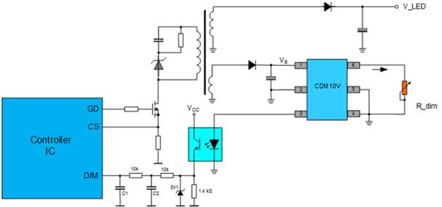
Fig. 2: Dimming Interface IC with Optocoupler
Successful implementation of an IC interface for dimming control is based on the ability to vary device parameters to suit design requirements. The variables include resistor current, frequency of the PWM signal and minimum duty cycle. In some designs, true dim-to-off functionality may be specified in order to minimize latent light output at the lowest dimming level and the risk of LED “pop” when the current is increased. In the past, any changes to these parameters would require extensive redesign of the circuit. User configurable settings in the IC allow for modification to these key parameters using a standard UART interface. This provides the flexibility to use a basic design across multiple fixtures or accommodate changes in other components, such as the optocoupler, without a re-engineering effort. The IC’s default settings (Table 1 ) are one-time only configurable using a programming board to set desired values.
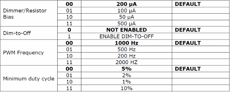
Table 1: Configurable parameters of CDM10V dimming interface IC
One of the most frequent variations in design revolves around the selection of a suitable optocoupler to balance performance, cost and reliability of the fixture. The most cost-effective solution is four-pin device consisting of an LED and a photo-sensitive BJT, with only the collector and emitter of the BJT connected to the pins. This simple 4-pin device has relatively low switching times. To meet higher speed requirements, a six-pin device where the base of the BJT is also connected to a pin may be used. When applications call for very high reliability and performance, a CMOS-based isolator may be used.
In many optocoupler configurations, the output signal is derived from the collector of the BJT, which results in an inverted signal compared to the original input. An additional inverter stage would be needed to produce a properly oriented signal to the controller IC. But as shown in Figure 2, with a sufficiently high Vce the BJT can be viewed as a current controlled source with no inversion of the signal.
There are two parameters of the optocoupler to consider in selecting the right device for this application. These are current transfer ratio (CTR) and the switching times (Tr and Tf ). The latter are data sheet values available from the device manufacturer. While Tr is fairly constant across the range of load resistance (RL ), Tf increases at a linear rate. CTR is the ratio between forward current of the LED (which is commonly specified at 5 mA) and resulting collector current of the optocoupler phototransistor. This ratio can vary as a function of both LED current and temperature across a range of 50% to 600%, which translates to current-controlled source output of the BJT ranging from 2.5 mA to 30 mA.
The relationships between CTR and switching times lead to the following guidelines for optocoupler selection. It is advisable to use the lowest PWM frequency that yields the targeted dimming response. The selected device should have a CTR range of 1:2. Load resistance should allow the desired output voltage at the lowest possible CTR over all possible operating conditions. Use a supply voltage (Vcc) at least 2 V higher than the target output. However, supply voltage should not be too high so as to limit power loss at the optocoupler stage. Finally, a Zener diode is useful to limit and stabilize the output voltage. The configuration of the optocoupler shown in Figure 2 is based on these guidelines.
At costs in the range of 50 cents or less, using an optocoupler instead of a transformer in the LED supply lowers material costs and the assembly cost for end devices. It also contributes to board space reduction of up to 70%, creating opportunities for form factor innovation in new fixtures and controls. In short, silicon integration of the dimming interface in LED fixtures serves to create opportunities for breakthrough designs that realize the promise of LEDs in lighting.
Advertisement
Learn more about Infineon Technologies


