A breakthrough in two-dimensional material by researchers at the University of Warwick could mean big things for the size and efficiency of all things tech. Dr. Neil Wilson in the Department of Physics is responsible for creating a new way to measure electronic structures of stacks of 2D materials that are thin, very conductive, flat, and strong.
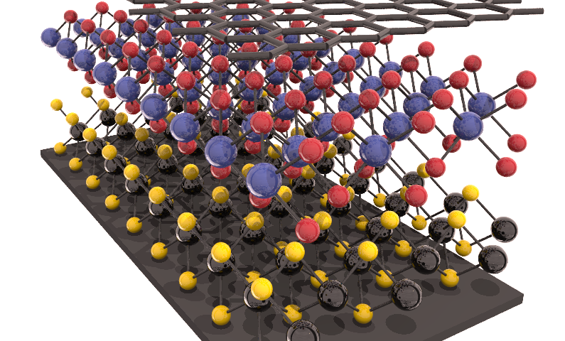
Heterostructures, or stacked layers of 2D materials, create optoelectronic devices with ultrafast electrical charge that are also highly efficient. These can be used in nano-circuits and are stronger than the types of materials used in typical circuits. By using a variety of 2D materials, heterostructures of many types have been created. By stacking different combinations of 2D materials, new materials with new properties have emerged.
The technique discovered by Dr. Wilson and his team measures the electronic properties of each of the stack’s layers, which allows researchers to discover the most optimal structure that will ensure the quickest, most efficient transfer of electrical energy. Dr. Wilson’s technique uses the photoelectric effect to measure the momentum of electrons within each layer, showing the changes when and where the layers combine.
“It is extremely exciting to be able to see, for the first time, how interactions between atomically thin layers change their electronic structure. This work also demonstrates the importance of an international approach to research; we would not have been able to achieve this outcome without our colleagues in the USA and Italy,” said Dr. Wilson.
The development of highly efficient nano-circuitry, as well as the creation of better, more flexible, smaller wearable gadgets, is made possible by the discovery and implementation of semiconductor structures that work efficiently, which requires a thorough understanding of how 2D heterostructures work. And these developments may have greater implications — solar power could be bettered through the use of heterostructures.
The material has thin layers that allow for strong absorption and efficient power conversion with a minimal amount of photovoltaic material, which allows for a kind of flexibility necessary for serious innovations.
Dr. Wilson worked with researchers in theory groups at the University of Warwick, the University of Cambridge, the University of Washington in Seattle, and the Elettra Light Source in Italy. Dr. Nick Hine from Warwick’s Department of Physics also helped the team to understand how the interactions between layers of atoms changed electronic structure.
Image: University of Warwick
Source: Phys.org
Advertisement
Learn more about Electronic Products Magazine


