BY KURT SHULER, Vice President of Marketing
ArterisIP
www.arteris.com
Back-end timing closure for on-chip SoC interconnects is now a significant obstacle for engineers who are migrating to smaller semiconductor geometries and FinFET transistors. So the industry needs to summon its innovative resources to address an issue that is now adding weeks, and even months, of delays to project schedules.
Perhaps the best path forward is to assign a higher priority to the interconnect earlier in the SoC planning stages. So the connections between IP blocks get designed for optimal functionality, location, performance, latency, power, and area before the front-end design migrates to the physical back end of the process.
In fact, design teams that commit to interconnect topology optimization during the front-end design have slashed more than 30 days from their schedules. This new path stands in contrast to the traditional treatment in which engineers throw interconnect RTL “over the wall” late in the process and let back-end synthesis-place-and-route (SP&R) engineers try to resolve the issues.
Timing failures worsen
Problems with interconnect timing closure first started popping up at the 28-nm process node, but now, at the 16-nm FinFET node, issues have become more common and acute. Migration to 10-nm and 7-nm processes will increase the number and significance of issues.
As transistors get smaller with each successive process node, chips are getting denser. Processor speeds have increased, but the interconnecting wires that link all of the IP blocks together have grown more congested and longer in length. Therefore, while the number of IP blocks in each design has ballooned, wire RC constraints have created more limitations.

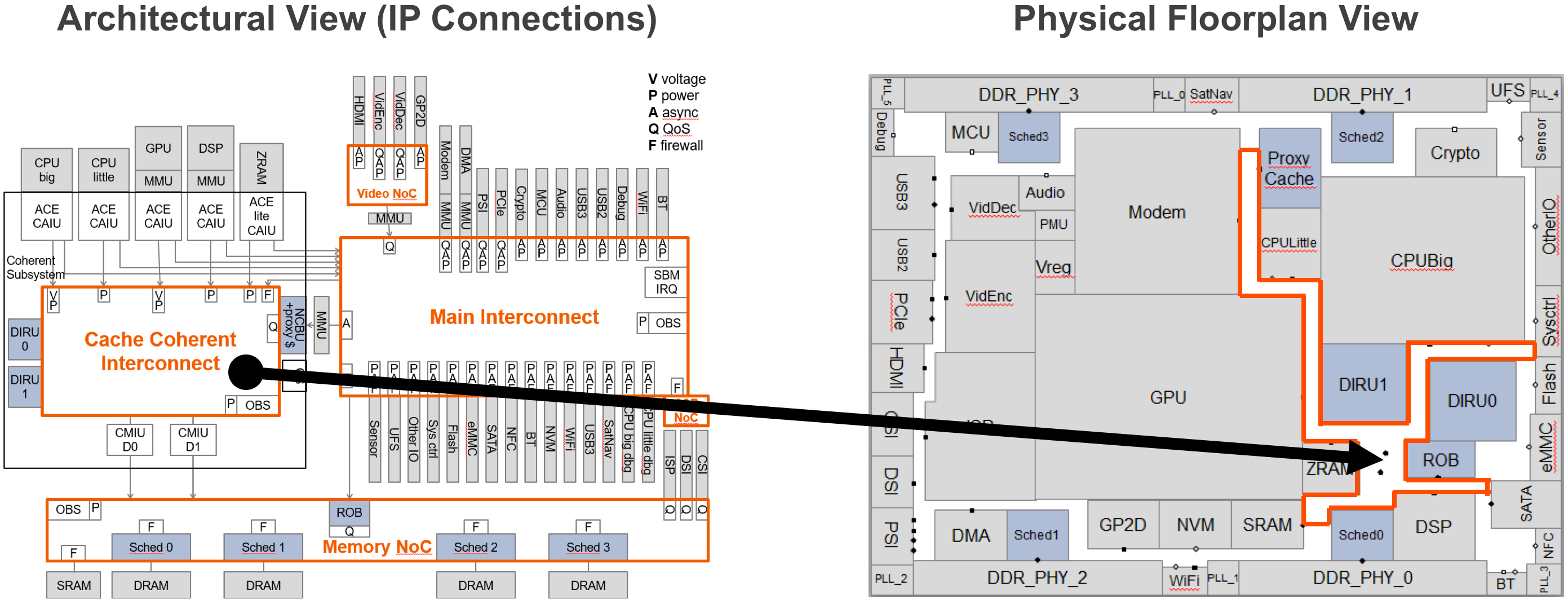
Fig. 1: Obtaining floorplan information earlier in the SoC design process helps discover interconnect timing closure issues sooner.
The interconnect has the longest wires of any SoC IP because it stretches across the chip like a spider web. It is also the last IP to be configured because it depends on all of the other on-chip IPs with which it connects.
Extended wire lengths combined with RC delays have made the interconnect one of the principal sources of timing closure issues, and even worse, these issues are usually not discovered until late in the design schedule. Waiting until the back-end stage to address these matters almost guarantees a schedule slip.
Planning for success
However, if designers could predict where timing issues might occur in the interconnect during the front end of the process, it’s possible that they could use that knowledge to create a design that avoids many problems that are popping up in greater numbers today.
Using this information up front will create better timing paths in the back end. With fewer issues to resolve, a more predictable SoC delivery schedule can be accomplished alongside the opportunity for additional benefits like higher overall performance, reduced die size, and lower power.
Interconnect issues need to be tackled when all IP blocks are placed from a functional and logical perspective rather than waiting for a final physical floorplan. This step traditionally occurs when the RTL design process is completed and locked in.
Because topology placement has traditionally come after this process, the interconnect IP gets constricted into suboptimal connection paths. However, if designers feed the process with greater information and planning during the front end, it enables better decision-making for the place-and-route tools implementing interconnect.
Critical intervention points
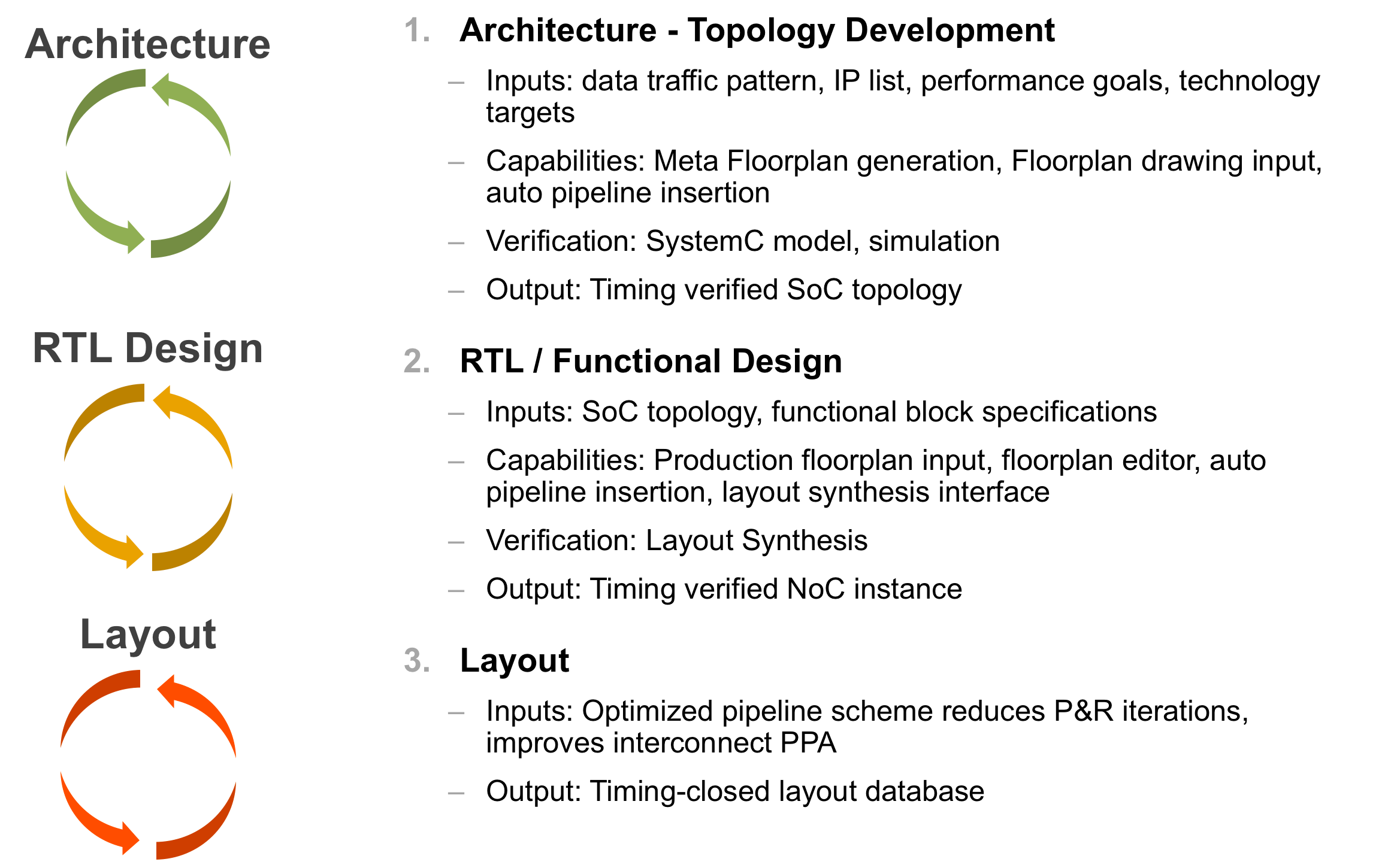
There are three steps in the design process in which timing issues can be initially detected and addressed: 1) in the SoC architecture and topology stage; 2) in the functional or RTL design stage; 3) and during the layout stage. After each stage, engineers simulate their designs and uncover and fix interconnect timing issues.
In today’s most sophisticated designs, timing issues that are detected in the SoC architecture take the least amount of time to resolve. By contrast, timing issues found in the functional or RTL stage can take days to resolve, while problems found in the layout stage take several weeks to rectify.

Fig. 2: It is better to find and fix timing closure issues at the earliest stages of SoC design.
Because schedule delays can weaken a project’s market viability, perhaps the best opportunity to address failed timing paths before they happen is at the RTL stage.
Finding timing issues in the netlist or afterward contributes to schedule delays. As the SoC design shifts to the physical design team, timing issues trigger problems that force the project back to front-end engineers who need to revise their plans to fix the structural problems.
Engineering change orders (ECOs) present an optional resolution path to edit the netlist created by front-end teams. However, innovative designers can emphasize forethought and advanced planning to devise an intelligent topology that will avert back-end errors that delay project delivery.

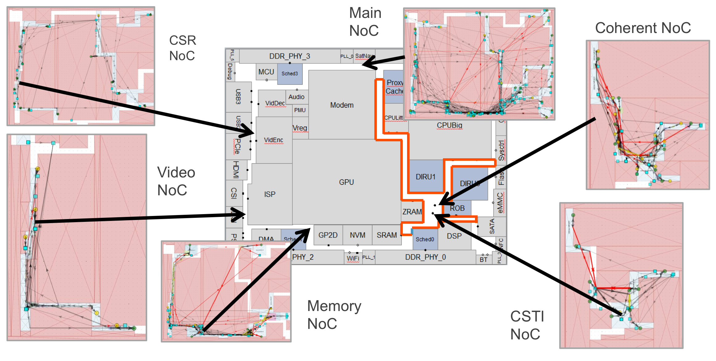
Fig. 3: This methodology works for the entire SoC and all of its interconnects.
The case for earlier interconnect timing closure
Designers that consider interconnect IP during the RTL and functional design phase will be in a better position to create low-latency connections and determine the ideal placement of interconnect components like network interface units, switches, gates, and other logic. Doing so creates the ideal conditions that promote the best performance, reduced logic footprint, fewer pipeline insertions, and a reduction in failed timing paths.
From a practical technology standpoint, when optimal interconnect placement gets factored into front-end design, engineers are given a better opportunity to create optimal timing routes. In fact, designers should be able to obtain early versions of the SoC floorplan to analyze the interconnect design and pre-determine issues that might contribute to failed timing closure later in the design flow process.
A user interface that reports on potential failures at this stage is essential in automating the error-resolution process by feeding die location, performance, and timing information into the back-end place-and-route tools, allowing the back-end tools to lay out a more optimized design.
Putting more forethought into the SoC interconnect IP to avoid delays is important for developers who are forging ahead into sub-16-nm FinFET process technology. Delivering IP intelligence into the front end ultimately slashes time-to-market and results in a higher-performing SoC.
Advertisement


