By Warren Miller, contributing writer
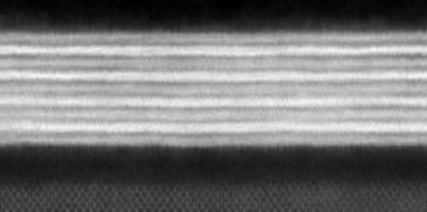
Just when you thought handheld electronic devices couldn’t get any smaller, a new breakthrough in semiconductor construction may be the key to miniaturizing technology even further. Researchers from the University of Chicago and Cornell University have collaborated on a method of making silicon films that are only as thick as a few atoms, allowing them to be stacked on top of one another many times over. Imagine a stack of Post-It notes, one layered on top of the other. By stacking microscopic sheets of semiconductors in such a way, scientists and engineers may be able to make smaller, more powerful versions of everything from personal electronic devices to solar-powered batteries.
Until now, these layers of silicon film were grown on top of one another, limiting the materials that they could be made with. The process of “growing” these layers requires materials that can withstand extremely high temperatures. This new method doesn’t require heat, as the layers are constructed individually and then laid down on top of one another. Instead of the layers being connected by strong covalent bonds, they’re connected with weaker bonds, allowing the integrity of their individual surfaces to remain intact.

The new method allows scientists to craft individual tiny films, each a few atoms high, and stack them for new types of electronics. Image source: UChicago Creative.
The ability to create layers of silicon films, atoms thick, may make it possible to shrink just about everything electronic. Imagine alternating layers of conductors and switches into three-dimensional electronic components or perhaps entire systems. Micro-machines could be included in the layers to provide sensors and actuators all on a single device. Without the need to drive signals off, chip power goes way down and performance goes way up. The possibilities are mind-boggling.

With layers of silicon films, the possibilities are endless. Image source: University of Chicago.
This method does come with its own set of problems, however. Because the layers themselves are only a few atoms thick, laying them down on top of one another precisely can be challenging. “The scale of the problem we’re looking at is, imagine trying to lay down a flat sheet of plastic wrap the size of Chicago without getting any air bubbles in it,” said JiWoong Park, a UChicago professor in the Department of Chemistry, the Institute for Molecular Engineering, and the James Franck Institute, who led the study.
Still, this innovative process may lead to countless breakthroughs in more fields of technology and industry than you can imagine. As Park said, “We expect this new method to accelerate the discovery of novel materials as well as enable large-scale manufacturing.” While the idea of something so infinitesimally small revolutionizing manufacturing on a large scale may be counterintuitive, big things have been known to come in small packages; and packages don’t come much smaller than this one.
Advertisement
Learn more about Electronic Products Magazine


