• Eight 250 MHz, 16-bit A/Ds
• Eight wideband FPGA-based Digital Down Converters (DDCs)
• 64 multiband FPGA-based DDCs
• Jade Architecture with Xilinx Kintex UltraScale FPGA
• Navigator Design Suite for Streamlined IP Development
Pentek, Inc., introduced the newest member of the Jade™ family of high-performance data converter XMC modules based on the Xilinx Kintex Ultrascale FPGA. The Model 71132 is an XMC module featuring eight 250 MHz 16-bit A/Ds with eight wideband digital down converters (DDCs) and 64 multiband DDCs, all fully programmable.
The Model 71132 doubles the number of A/D channels and DDCs over previous models giving this the best price per channel ratio in the product family. Applications monitoring a broad spectrum with a need to quickly analyze specific portions of the identified spectrum can greatly benefit from the capabilities of the 71132.
Performance IP Cores
The 71132 factory-installed functions include eight A/D acquisition IP modules, each containing nine DDCs. In each module, the wideband DDC supports decimations from 2 to 32 for capturing signal bandwidths up to 100 MHz. The eight narrowband DDCs allow decimations up to 1024 for signal bandwidths down to 200 kHz. These two types of DDCs operating in parallel are ideal for applications that need to monitor a wide spectrum, but quickly tune to identified frequency bands of interest for further analysis.
“We continue to expand our factory-installed FPGA functions to boost DDC channel density and add new operational modes for our customers, right out of the box,” said Bob Sgandurra, director of Product Development of Pentek. “The Navigator FPGA Design Kit (FDK) includes a wealth of Pentek IP library modules so customers can easily add custom IP to support specific needs. The Model 71132 is a very cost effective solution for applications that need many DDCs to capture both wide and narrow frequency bands.”
The Jade Architecture
The Pentek Jade Architecture is based on the Xilinx Kintex UltraScale FPGA, which raises the digital signal processing (DSP) performance by over 50% with equally impressive reductions in cost, power dissipation and weight. As the central feature of the Jade Architecture, the FPGA has access to all data and control paths, enabling factory-installed functions including data multiplexing, channel selection, data packing, gating, triggering and memory control. A 5 GB bank of DDR4 SDRAM is available to the FPGA for custom applications. The x8 PCIe Gen 3 link can sustain 6.4 GB/s data transfers to system memory. Eight additional gigabit serial lanes and LVDS general purpose I/O lines are available for custom solutions.
Navigator Design Suite for Streamlined IP Development
Pentek's Navigator Design Suite consists of two components: Navigator FDK (FPGA Design Kit) for integrating custom IP into Pentek sourced designs and Navigator BSP (Board Support Package) for creating host applications. The FDK includes the board’s entire FPGA design as a block diagram that can be edited in Xilinx’s Vivado tool suite. In addition to the block diagrams, all source code and complete IP core documentation is included. Developers can integrate their own IP along with the Pentek factory-installed functions or use the Navigator kit to completely replace the Pentek IP with their own.
The Navigator BSP is a complete library of software functions for operation of the board. Each hardware and IP functional block included in the board’s architecture has an associated software module for controlling that function. This one-to-one mapping between software and hardware makes writing applications for the board more intuitive and simplifies the task of updating software to control new, user created FPGA IP functions. The BSP includes a collection of sample applications and a full-featured signal analyzer tool that displays data in time and frequency domains. The Navigator BSP is available for Windows and Linux operating systems.
Pre-Configured SPARK System Ready for Immediate Use
With a Pentek 8266 SPARK® PC, 8264 SPARK 6U VPX, or 8267 SPARK 3U VPX development system, work can begin immediately on applications. A SPARK system saves engineers time and expense associated with building and testing a development system and ensures optimum performance of Pentek boards. SPARK development systems are ready for immediate operation with software and hardware installed. In many applications, the SPARK development system can become the final deployed application platform.
Form Factors
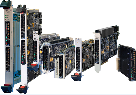
The Model 71132 XMC module is designed to operate with a wide range of carrier boards in PCIe, 3U & 6U VPX, AMC, and 3U and 6U CompactPCI form factors, with versions for both commercial and rugged environments.
Pricing and Availability
Designed for air-cooled, conduction-cooled and rugged operating environments, the Model 71132 XMC module with 5 GB of DDR4 SDRAM starts at $16,745 USD. Additional FPGA options are available. Delivery is 8 to 10 weeks ARO.
Advertisement
Learn more about Pentek


