By Nazzareno (Reno) Rossetti and ChiYoung Kim, Maxim Integrated
High-performance multicore CPUs with integrated graphics processing units have made their way into smartphones. Smartphones now carry capabilities that we used to expect from high-end audio/video equipment and desktop computers. Today’s smartphones have 4K video capture, high-end gaming, program multitasking, virtual reality functions, and higher display resolution.
While these are great features from the user’s perspective, they require large amounts of computation, resulting in high system power consumption that generates a lot of heat. To compound this problem, the hardware must fit volumetrically into small form factors, making it difficult to dissipate that heat. This article reviews a solution to address the challenges of feeding the smartphone’s power-hungry processors.
Fig. 1: CPU core chip for smartphones and tablets.
More power to the buck converter
In relation to the trends outlined above, the buck converter that powers these processors has evolved from a single-phase device that delivers a few hundred milliamperes of current to a multiphase device that can successfully deliver over tens of amperes of current. Even so, a state-of-the-art smartphone typically has a battery capacity slightly above 2,000 mAh. This means that if it consumed a single ampere of continuous current, it would last only two hours, let alone the widely expected full day of operation. The magic then resides in strict power and thermal management that minimizes wasted power and controls temperature rise by delivering the necessary power peaks when required and immediately retreating into low-power modes of operation.
- The thermal challenge
As an example, a PCB-mounted processor with a junction-to-ambient thermal resistance R = 50°C/W and a thermal capacitance C = 6 Joules/°C, under a power pulse P = 10 W (10 A x 1 V), would experience a temperature rise, given enough time, by a clearly unacceptable amount ΔT = R x P = 50 x 10 = 500°C. However, if the power pulse is limited in time — for example, t = 60 s — then the temperature rise is damped by the effect of the RC constant and is limited to a more acceptable ΔT ≈ t x P/C = 60 x 10/6 = 100°C. The linear approximation for ΔT is valid for t e−t/RC
- The efficiency challenge
Accordingly, a switching regulator IC with a thermal resistance R = 60°C/W and a thermal capacitance C = 4 Joules/°C, delivering a 10-W power pulse at efficiency η = 85%, will dissipate the power P = (1-η) x P = 0.15 x 10 = 1.5 W. Assuming that all of the losses can be attributed to the IC, given sufficient time, its temperature would rise to ΔT = R x P = 60 x 1.5 = 90°C above the ambient temperature. However, after 60 s, the temperature would rise only by ΔT ≈ t x P/C = 60 x 1.5/4 = 22.5°C.
Naturally, the higher the efficiency, the lower the losses that the voltage regulator will incur and the lower the temperature rise.
- The power of accuracy
A voltage regulator delivering 0.9-V output with ±1% accuracy to a resistive load Rr at +1% error will deliver 2% excess power (V2 /Rr). That is the same as taking the efficiency curve and lowering it by two percentage points! Accuracy saves power.
- The power of fast transient response
The output of a slow voltage regulator will dip under a positive transient load and will need to be positioned higher to assure that the load receives the minimum voltage necessary to operate. Similar considerations are valid for a regulator that exhibits high voltage ripple. In both cases, this results in wasted power and greater heat generation, ultimately ending in less battery life. Fast transient response and low ripple save power.
- The size challenge
As discussed earlier, a large amount of power must be packed into the small volume of a smartphone. Accordingly, the buck converter must be accurate, fast, and efficient to minimize power losses. Efficiency must also be maintained while operating with high clock rates to reduce the size of the passive components (output inductors and input/output capacitors).
Quad-phase buck converter
The MAX77874 16-A, quad-phase, buck regulator (Fig. 2 ) can be used to manage the challenges outlined above. Dividing the current between four phases that are equally spaced in time across one clock period has several advantages compared to a single-phase architecture.
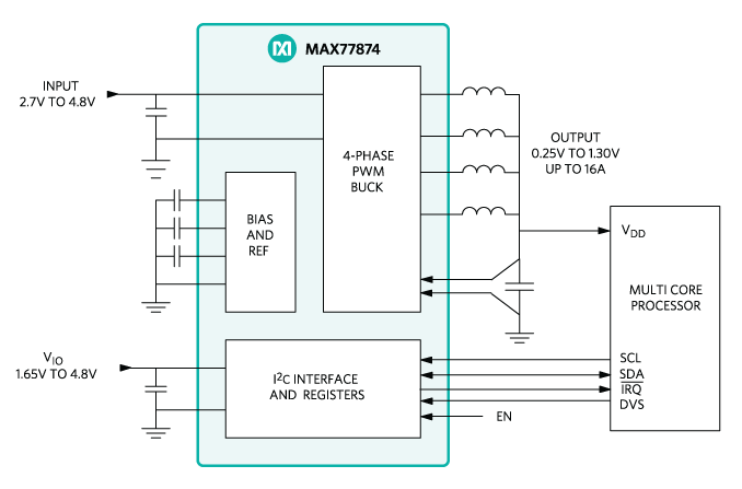
Fig. 2: MAX77874 quad-phase block diagram.
First, the four interleaved phases assure ripple current cancellation as shown in Fig. 3 . Low total ripple current is obtained at a relatively per-phase low frequency of operation. Lower ripple current means that fewer capacitors are needed on the output, resulting in a smaller bill of material (BOM).
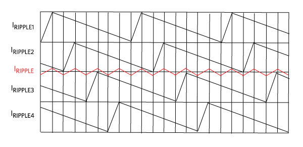
Fig. 3: Quad-phase output current ripple cancellation.
Second, the multiphase architecture results in the need for fewer input capacitors. Fig. 4 shows the VLXA -to-VLXD voltage waveforms applied to the inductors in forced pulse-width-modulation (PWM) mode. This can also be viewed as a representation of the pulses of current drawn at the input by each inductor during the “on” time. The total input current is the sum of the four out-of-phase currents. Here, spreading the total input current over time reduces the input current total RMS value compared to single-phase operation, allowing for a smaller input current ripple filter.
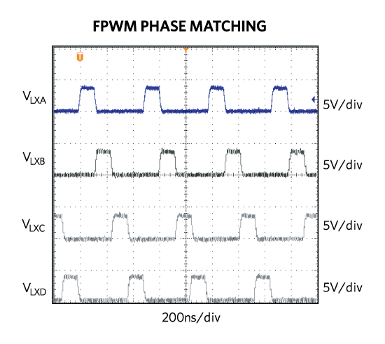
Fig. 4: Quad-phase LX voltage waveforms.
Third, a multiphase scheme is more efficient than a single-phase scheme. The latter, by running at four times the frequency of the quad phase, can also achieve low ripple but at higher switching losses. The two schemes have an equal number of transitions within one period, but the quad-phase converter transitions carry a quarter of the current of the single-phase converter.
The MAX77874 also provides several enhancements, including an adaptive on-time control loop and turbo skip mode.
The MAX77874 features an adaptive on-time control loop, which is an enhanced version of the popular, fast-response, constant on-time control. The adaptive scheme results in pseudo-constant frequency in a scheme that otherwise would have variable frequency, which can be problematic in noise-sensitive applications. This mode of operation is also known as forced PWM (FPWM) mode. The compact 48-bump, 0.35-mm pitch WLP array package also requires minimal PCB area.
During a heavy load transient, the four phases move from interleaved to parallel operation. Paralleling the four phases results in the fastest possible load current step response because the four inductor currents are concurrently delivered to the load. In Fig. 5 , the buck converter operates in FPWM mode at any load and during the transition from light to heavy load.
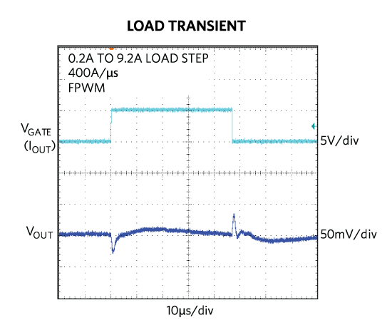
Fig. 5: FPWM transient response.
Turbo skip mode combines superior transient response with light-load efficiency. At light loads and when enabled, the MAX77874 turbo skip mode (Fig. 6 ) keeps all four phases operating sequentially but at a lower quiescent current and variable frequency. This is known as rotational phase spreading.
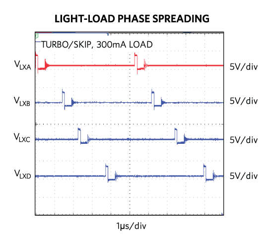
Fig. 6: Light-load rotational phase spreading.
This way, during a transition from light to heavy loads, there is no delay in activating all four phases and the MAX77874 performs as well as it does in FPWM mode (shown by comparing Fig. 5 with Fig. 7 ).
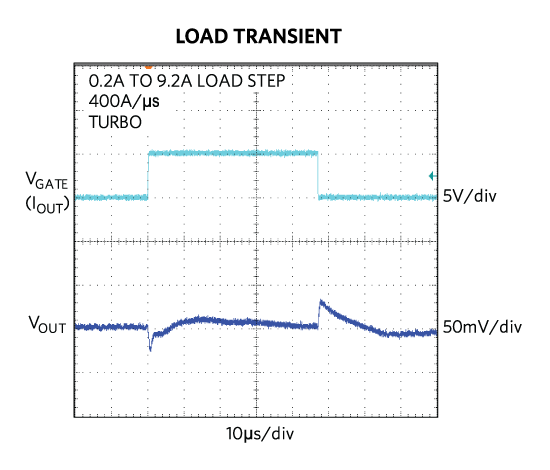
Fig. 7: Turbo skip mode transient response.
Compared to phase shedding — turning off some of the four phases at light loads — this scheme produces less output ripple and has fewer glitches. Fig. 8 shows that with rotational phase spreading, the output voltage ripple is less than 3 mVP-P from 0 to 500 mA. The turbo skip mode is the default mode of operation at light loads.
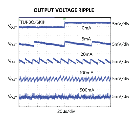
Fig. 8: Output voltage ripple with phase spreading .
Regular skip mode provides the lowest supply current and highest efficiency at light loads, although with slightly slower response. The modes of operation can be programmed through the I2 C bus.
With an initial output accuracy of ±2.5 mV (±0.25% at 1-V output) and outstanding performance over temperature, line, and load regulation, the MAX77874 has the best output accuracy. Fig. 9 shows the initial output accuracy versus the setting in skip, turbo skip, and FPWM modes.
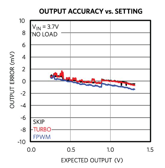
Fig. 9: Output voltage initial accuracy vs. setting.
In addition, the enhanced features of the MAX77874’s integrated power MOSFETs result in superior efficiency compared to competitive quad-phase solutions. The efficiency comparison in Fig. 10 shows that the MAX77874, even with a smaller 2012 inductor, has an advantage of up to 4% versus a competitive device.
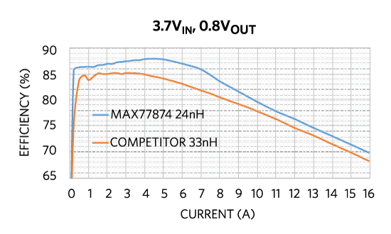
Fig. 10: Efficiency comparison.
The MAX77874 application requires only a small 37-mm2 area when placed on a PCB (Fig. 11 ), an overall 29% size advantage compared to a competitive solution.
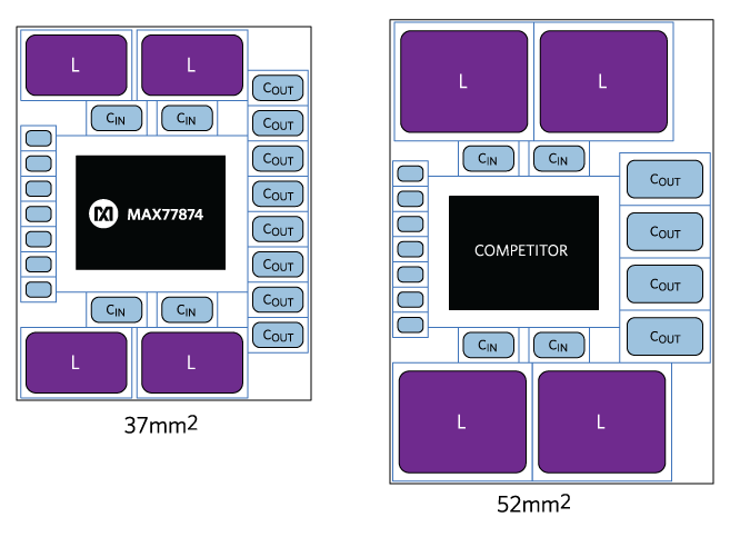
Fig. 11: MAX77874 size advantage.
Conclusion
The MAXX77874 is well-suited to address the power and thermal management requirements of increasingly powerful CPUs and GPUs in smartphone designs. It provides industry-leading transient response, output voltage accuracy, and high efficiency in a small PCB footprint.
About the authors
Nazzareno (Reno) Rossetti, Ph.D. EE at Maxim Integrated, is a seasoned analog and power management professional and a published author who holds several patents in this field. He has a doctorate in electrical engineering from Politecnico di Torino, Italy.
ChiYoung Kim is a director of the Product Definition and System Engineering Group in the Mobile Power business unit at Maxim Integrated. He has more than 20 years of experience in the power electronics and semiconductor industry. ChiYoung holds a Bachelor’s degree in electrical engineering from Inha University, South Korea.
Advertisement
Learn more about Maxim Integrated


