Editor's Note: Welcome to AspenCore’s Special Project on Embedded Artificial Intelligence (AI). This article, along with the articles listed on the last page, form an in-depth look from a variety of angles at the business and technology of imbuing embedded systems with localized AI.

By Gina Roos, editor-in-chief, Electronic Products
Developers and systems designers have a number of options available to them for adding some form of neural-networking or deep-learning capability to their embedded designs. Early on — and even today — designers have successfully used graphics processing units (GPUs) and field-programmable gate arrays (FGPAs), both of which dovetailed nicely into the memory-intensive demands of deep learning. Even traditional x86 CPUs have found their way into AI applications.
Many developers have discovered that these existing technologies aren’t always the best fit. As a result, over the past few years, a number of startups (as well as established chipmakers) are focused on building chips specifically for AI applications. These chips are built from the ground up to meet the computing power needs for AI algorithms and running applications.
It is important to note that IP blocks for SoCs are another option for providing neural-network functionality, but that is another story. Vendors in this space include Cadence, Ceva, NXP, Synopsys, and VeriSilicon.
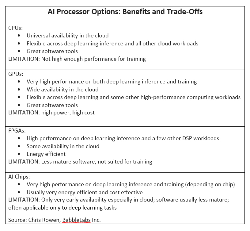
But like all technologies, there are advantages and trade-offs to every solution. Overall, designers need to choose the best technology based on their specific end application. AI chips are typically segmented into three key application areas — training on the cloud, inference on the cloud, and inference on the edge.
The big gun in training is Nvidia’s GPU, which has become a popular choice for training machine-learning algorithms. This process analyzes trillions of data samples. A big advantage here is the GPU’s parallel computing architecture.
Inference on the cloud tackles machine-learning models for many AI applications that are too compute-intensive to be deployed on edge devices. Processors such as FPGAs that can deliver low latency and handle compute-intensive tasks offer advantages in these applications. Because not all computing tasks for AI features can be done on the cloud, chipmakers — both existing and startups — are developing their own AI chips and adding AI features to their processors.
So what are the first questions that designers need to answer before dipping their toes into the AI waters? I spoke with Silicon Valley entrepreneur and technologist Chris Rowen, CEO of BabbleLabs Inc . and Cognite Ventures, to get a few answers.
Question 1: Know your end-application requirements
When starting out on any design, the first question is always what your end-application requirements are. This is followed up by “Do I have one specific task in mind?” and sometimes that is very clear, said Rowen. “If I’m a systems designer building a security camera, I’m going to care a lot about how well the chip runs a cross-section of video streaming — object detection, object recognition, object tracking, etc. – a handful of tasks that are specifically related to that end application.”
The next question is if the application will run in the cloud or in an edge device. This will drive designers into different directions in terms of what chips they should consider.
“The end application is clearly important,” said Rowen. “If it’s in the cloud, the question will be, ‘Is it going to be used for training neural networks or only for inference?’ — running a previously trained network. If it’s on the edge, what are the set of specific applications that you want to run?”
Rowen said that most new chips are being built for vision applications on the edge, which are primarily used in inference applications for one flavor or another for imaging or video analysis. A growing sub-category that is increasingly becoming important is audio, especially for voice processing.
So it comes down first to cloud versus edge. Then within cloud, is it training or inference? Within edge, is it general-purpose (where the application is unknown) versus vision or some other specialized application like speech processing?
Question 2: Software support
Software tools also help distinguish between the different chips. “If it is a training chip, does it support a variety of training environments — TensorFlow, PyTorch, and others — because there are a number of important training environments that application and software development teams use,” said Rowen. He said that Nvidia is the gold standard and the dominant supplier of training silicon today.
“On the inference side, it’s a question of how well you can take a pre-trained model and map it down to the particular characteristics of the chip. That’s an easier question when there are standards like the Neural Networks Exchange Format.” NNEF is a standard promoted by the Khronos Group to make it easier to standardize mapping tools.
“Typically, the complexity of these neural networks is not as great compared to all the other software involved in mapping an application onto some new processing engine,” explained Rowen. “Even if the tools aren’t perfect, people can usually find a way to do that mapping of an existing neural network down onto a vision chip or audio chip or whatever the edge-processing silicon is with less sophisticated tools.”
In cases in which software plays a less central role — and even when it does play a key role — designers should look at the price, performance, and power efficiency at the hardware level, which brings up the next set of questions.
Question 3: Memory requirements
The perennial questions for any chip selection revolve around cost and performance. And for neural networks, what is the on-chip memory and how much memory bandwidth does the chip provide?
“Some of these neural network problems are very memory-intensive,” said Rowen. “Certainly the training process, which is usually taking place in the cloud, is very memory-intensive, requiring both significant on-chip memory and very high memory bandwidth.”
The inference process is usually much less memory-intensive and may not require a lot of off-chip bandwidth depending on the target application, he added.
So here’s the challenge. One of the things that distinguishes between chips built for general-purpose and a specific application is whether the chip designers have allocated a lot of resources to on-chip memory and off-chip memory bandwidth. However, if the designers don’t know which applications they need to run, they will likely need to over-provision in terms of memory bandwidth, which makes it more expensive.
“Over-provisioning will add cost, which is why general-purpose is almost always more expensive than special-purpose chips — because they have to buy a bigger insurance policy,” said Rowen. Trade-offs can include cost, power, and physical footprint.
If a designer can narrow the requirements a little bit so that a lower cost and lower-power chip will fit the application, then there can be a big step up in performance at the system level, said Rowen. “The difference between general-purpose and special-purpose [chips] can be an order of magnitude.”
Question 4: Performance — latency versus throughout
The ultimate definition of performance is how fast the chip runs in the neural-network application. The two relevant metrics here are throughput and latency — whether the system is optimized for increasing throughput or optimized for reducing latency.
In the cloud, the emphasis is typically on throughput, while latency tends to be very important in real-time edge systems, said Rowen. For example, if you’re building a chip for an autonomous driving application, latency is more important — and is a critical safety issue, he added.
“Fortunately, for many of these neural-network applications, there is quite a strong correlation between the delivered performance and the multiply rate of that chip,” explained Rowen. “There is some variation in how well-utilized the computational resources are, but at the simplest level, just asking ‘how many multiply-accumulates per second at a given resolution’ or ‘how many multiply-accumulates per watt’ a chip does is a pretty good rough guide to the capability of a chip.”
Today, in general, GPUs are the reigning force for neural-network training in the cloud, and plain x86 processors are the most common platform for inference in the cloud because they have the flexibility to run the complete application that includes deep-learning elements and conventional software elements on a single processor, said Rowen.
For the most part, there isn’t much training taking place on the edge; it’s focused on inference typically for specific use cases like video or audio, he added.
Rowen provided Electronic Products with a rough assessment of where some chips (from startups and existing platforms) are positioned by application. “There is a trend that chips targeting the cloud are more general-purpose and chips targeting the edge are more specialized.”
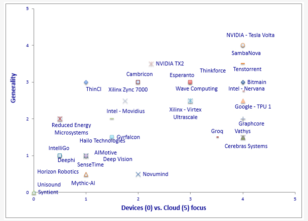
On the x-axis: 0 means most adapted to edge devices (car, phone, IoT); 5 means most adapted to the cloud. On the y-axis: 0 means narrowly specialized to neural networks, especially neural-network inference; 5 means general-purpose, spanning neural-network inference, training, and other non-neural-network (but compute-intensive) applications. Image Source: Cognite Ventures LLC.
Here is a snapshot of some AI-enhanced chips and platforms that provide a hint of the variety of neural-networking solutions available in the market today across mobile and enterprise applications:
Gyrfalcon’s Lightspeeur AI chip : Startup Gyrfalcon Technology Inc. touts an ultra-low-power and high-performance AI chip. The Lightspeeur 2801S intelligent matrix processor is based on the APiM architecture that uses memory as the AI processing unit. “This eliminates the huge data movement that results in high power consumption, enabling a superior energy efficiency at 9.3 TOPS [tera operations per second]/watt,” said the company. “The architecture features true, on-chip parallelism, in situ computing, and eliminates memory bottlenecks. It has roughly 28,000 parallel computing cores and does not require external memory for AI inference.”
The company claims that the arithmetic logic unit (ALU) usage efficiency is 77% and higher running convolutional neural networks (CNNs).
Turnkey reference designs are available, including for USB dongles, multi-chip boards, and system development kits. Target applications include mobile edge computing, AI-based IoT, consumer portable devices, smart surveillance video, AR/VR products, face detection/recognition, natural language processing, deep-learning-enabled devices, AI data center servers, and autonomous driving.
Huawei’s Kirin 970 : HUAWEI Consumer Business Group’s first mobile AI computing platform, featuring a dedicated neural processing unit (NPU), combines cloud AI with native AI processing. The Kirin 970 is comprised of an eight-core CPU and a new generation 12-core GPU.
“Compared to a quad-core Cortex-A73 CPU cluster, the Kirin 970’s new heterogeneous computing architecture delivers up to 25x the performance with 50x greater efficiency,” said HUAWEI. Translation: The chipset delivers the same AI computing task faster with less power. A benchmark image-recognition test shows that the Kirin 970 processed 2,000 images per minute.
In addition to using the new AI chipset in its own phones, HUAWEI is positioning the mobile AI as an open platform, offering the technology to developers and partners.
Intel’s Nervana neural-network processor (NPP): Claimed as the industry’s first silicon for neural-network processing, the Nervana NNP, introduced late last year, was three years in the making. Purpose-built for deep learning, the Intel Nervana NNP does not have a standard cache hierarchy and on-chip memory is managed by software. “Better memory management enables the chip to achieve high levels of utilization of the massive amount of compute on each die,” said Intel. “This translates to achieving faster training time for deep-learning models.”
In addition to a new memory architecture, Intel also developed a new numeric format, Flexpoint, which provides a significant increase in parallelism on a die while decreasing power per computation. Because neural-network computations on a single chip are largely constrained by power and memory bandwidth, said Intel, Flexpoint delivers a higher degree of throughput for neural-network workloads. Intel’s goal with the new design was to “achieve high compute utilization and support true model parallelism with multichip interconnects.”
Intel’s Movidius VPUs : Intel is working with Microsoft to enable AI inference at the edge, combining Microsoft Windows ML with Intel’s Movidius vision processing units (VPUs). A purpose-built chip for accelerating AI workloads at the edge, the Intel Movidius Myriad X VPU claims to be the industry’s first system-on-chip shipping with a dedicated neural compute engine for hardware acceleration of deep-learning inference at the edge. “This third-generation VPU is specifically designed to run deep neural networks at high speed and low power to offload specific AI tasks from burdening other hardware,” said Intel.
Intel also continues to optimize its Xeon scalable processors and data center accelerators for general-purpose machine learning and inference workloads.
MediaTek Inc.’s NeuroPilot AI platform : Designed for AI edge computing, the NeuroPilot platform offers a combination of hardware and software, an AI processing unit, and NeuroPilot software development kit (SDK). It supports mainstream AI frameworks including Google TensorFlow, Caffe, Amazon MXNet, and Sony NNabla and at the OS level supports Android and Linux.
MediaTek said that the platform “brings AI closer to the chipset level — for devices at the edge of computing — where deep learning and intelligent decision need to happen faster,” creating a hybrid of an edge-to-cloud AI computing solution.
Nvidia’s Tesla V100 GPU : Nvidia boosted its deep-learning computing platform with 10x better performance compared to the previous generation. The new NVIDIA Tesla V100 also includes a 2x memory boost (32 GB of memory) to handle memory-intensive deep learning and high-performance computing workloads and a new GPU interconnect fabric called NVIDIA NVSwitch. This enables up to up to 16 Tesla V100 GPUs to simultaneously communicate at a speed of 2.4 terabytes per second, said the company. Nvidia also updated the software stack. The Tesla V100 32GB GPU is available across the complete NVIDIA DGX system portfolio.
NXP’s machine-learning (ML) environment for edge processing : Proving that machine-learning models can be run on the edge with existing CPUs, NXP Semiconductors N.V. launched an embedded AI environment that allows designers to implement machine learning across NXP’s product portfolio from low-cost microcontrollers to the i.MX RT processors and high-performance application processors. The ML environment delivers turnkey enablement for selecting the right execution engine (Arm Cortex cores, high-performance GPUs/DSPs) and tools for deploying machine-learning models, including neural nets, on those engines, said NXP.
In addition, NXP said that the environment includes free software that allows customers to import their own trained TensorFlow or Caffe models, convert them to optimized inference engines, and deploy them on NXP’s processing solutions from low-cost MCUs to the i.MX and Layerscape processors.
“When it comes to machine learning in embedded applications, it’s all about balancing cost and the end-user experience,” said Markus Levy, head of AI technologies at NXP, in a statement. “For example, many people are still amazed that they can deploy inference engines with sufficient performance even in our cost-effective MCUs. At the other end of the spectrum is our high-performance crossover and applications processors that have processing resources for fast inference and training in many of our customer’s applications. As the use cases for AI expand, we will continue to power that growth with next-generation processors that have dedicated acceleration for machine learning.”
NXP also offers its EdgeScale platform for deployment from the cloud to embedded devices (IoT and edge). The company explained that EdgeScale containerizes “AI/ML learning and inference engines in the cloud and securely deploys the containers to edge devices automatically.” NXP also created an ecosystem of partners for ML tools, inference engines, solutions, and design services.
Qualcomm’s Snapdragon 845 : Qualcomm Technologies’ third-generation AI mobile platform is said to provide a 3x improvement in AI performance compared to the previous-generation SoC.
In addition to the existing support for Google’s TensorFlow and Facebook’s Caffe/Caffe2 frameworks, the Snapdragon Neural Processing Engine (NPE) SDK now supports Tensorflow Lite and the new Open Neural Network Exchange (ONNX), making it easy for developers to use their framework of choice, including Caffe2, CNTK, and MxNet, said Qualcomm. It also supports Google’s Android NN API. Target applications include smartphones, XR headsets, and always-connected PCs.
For security, the Snapdragon 845 now offers a hardware-isolated subsystem, the secure processing unit (SPU), which adds “vault-like characteristics to existing layers” to Qualcomm’s mobile security solutions.
Qualcomm’s AI Engine, comprised of several hardware and software components with on-device AI processing found on the Snapdragon 845, will be supported on Snapdragon 845, 835, 820, and 660 mobile platforms. The AI Engine supports Snapdragon core hardware architectures — Qualcomm Hexagon Vector Processor, Qualcomm Adreno GPU, and Qualcomm Kryo CPU. Software components include Snapdragon Neural Processing Engine, Android Neural Networks API, and Haxagon Neural Network.
Thanks to heterogenous computing, the Snapdragon 845’s new architectures deliver significant improvements. For example, Qualcomm said that the new camera and visual processing architectures deliver up to 30% power reduction for video capture, games, and XR applications compared to the previous generation, and graphics performance and power efficiencies deliver up to a 30% improvement as a result of the new Adreno 630 compared to the previous generation.
Samsung’s Exynos 9 series : Earlier this year, Samsung Electronics Co., Ltd., launched its latest premium application processor (AP), the Exynos 9 Series 9810 , for AI applications and richer multimedia content. This mobile processor is Samsung’s third-generation custom CPU (2.9 GHz) with an ultra-fast gigabit LTE modem and deep-learning-enhanced image processing.
The processor has a new eight-core CPU, four of which are third-generation custom cores that can reach 2.9 GHz with the other four optimized for efficiency. “With an architecture that widens the pipeline and improves cache memory, single-core performance is enhanced two-fold and multi-core performance is increased by around 40% compared to its predecessor,” said Samsung.
The chip also adds new features to enhance user experience with neural-network-based deep learning and stronger security via a separate security processing unit to protect personal data such as facial, iris, and fingerprint information. The Exynos 9 Series 9810 is currently in mass production.
These are only a few of the AI processor options currently or soon to come onto the market. By asking the four questions that Rowen outlined, however, developers will be able to zero in on the best candidates for their specific embedded AI project.
Want to dig deeper into embedded AI? Check out these other articles from AspenCore’s Embedded AI Special Project.
Artificial Intelligence (AI): Who, What, When, Where, Why? — These days, it seems like everyone is talking about artificial intelligence (AI), but what is it, who is doing it, and why is it important? (EEWeb)
Applying machine learning in embedded systems — Machine learning has evolved to become a practical engineering method if approached with a suitable appreciation of its associated requirements and current limitations — and it’s more accessible than you might think. (Embedded.com)
AI attracts chips to the edge — Virtually every embedded processor vendor has a product or is working on one for accelerating deep-learning tasks on client systems at the network’s edge. (EE Times)
AI Hardware Acceleration Needs Careful Requirements Planning — For optimum performance in embedded AI, use the most advanced single or heterogeneous processing architectures, but AI can be done quite ably using currently available kits. (EDN)
Other articles of interest:
Baidu Accelerator Rises in AI — China’s Baidu announced that it designed Kunlun, the latest of a growing crowd of deep-learning accelerators for training and inference jobs. (EE Times)
Addressing ‘Memory Wall’ is Key to Edge-Based AI — Addressing the “memory wall” and pushing for a new architectural solution enabling highly efficient performance computing for rapidly growing AI applications are key areas of focus for Leti, the French technology research institute of CEA Tech. (EE Times)
Engineer’s guide to embedded AI — Plenty of resources are becoming available to help engineers explore how to harness the new world of deep learning in their power-constrained designs. (Electronic Products)
Bringing machine learning to the edge: A Q&A with Neurala’s Anatoli Gorshechnikov — Practical application of machine learning at the edge brings multiple challenges, but one approach holds promise for fitting on resource-constrained devices without sacrificing accuracy. (Embedded.com)
Transfer learning for the IoT — Transfer learning is critical to the successful deployment of IoT deep-learning applications that require complex machine-generated information of such volume and velocity that it would be simply impossible to ever find enough human experts to label it and train new models from scratch in a reasonable amount of time. (Embedded.com)
Advertisement
Learn more about Electronic Products Magazine


