By Asem Elshimi, Design Engineer, RF-IoT, Silicon Labs
Disclaimer: This is not a technical introduction to soldering. Instead, I’m sharing my insights and personal experience with printed-circuit-board (PCB) soldering that have transformed my perception of the hours that I’ve spent in the lab as an IC designer.
I have been working in the semiconductor industry for the last seven years, yet I just finished my first soldering project last week. Why so long to get started? Because there was always someone in the lab who could solder for me. I also must admit that I was a late starter in soldering because I simply didn’t understand soldering basics. Outsourcing small tasks in the lab increases our efficiency and helps us focus on the big picture. But this is not true for soldering, in my opinion.
Long story short, as part of my training as a new hire at Silicon Labs , my project lead encouraged me to learn how to solder. Thus started, without exaggeration, a life-changing engineering experience. Soldering turns out to be an art. Or as the lab technician, who generously guided me through a starter project of soldering a tiny 0201 part to a reused PCB, told me the first time that I walked into his lab, “Soldering takes as much effort and passion as learning how to play the guitar.”

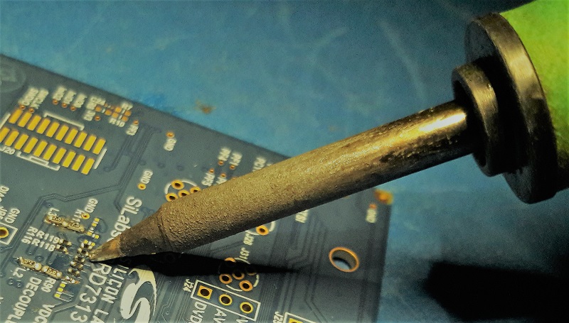
Fig. 1: An iron tip in contact with solder on one end of a capacitor in a 0402 package.

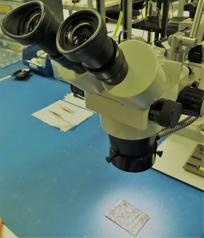
Fig. 2: My soldering mentor gave me the green light to use a microscope-equipped bench.
From there, I started my first soldering project. My soldering mentor gave me a practice PCB, an iron, tweezers (which need to be chosen depending on the size of the elements you plan to solder), solder wire, solder wick, and soldering flux — and, of course, some electrical elements to play with. Then he gave me the green light to use a bench equipped with a microscope.
Starting with zero experience, I spent the first half hour staring at the elements under the microscope. “So these are the matching elements that I have been simulating and measuring,” I said to myself. It was a moment of connection and a moment of reverse-alienation. The concepts, ideas, and theories that I had in mind about circuit elements were suddenly cast into a tiny spec of metallic packaging. An 0201 capacitor that is difficult to see even under the microscope is the material expression of our engineering knowledge and practices about capacitors.

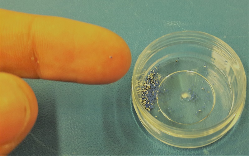
Fig. 3: 2.7-nH inductors in 0201 packages are difficult to see with the naked eye.
My first two trials of soldering elements to the board were disastrous. I covered the part with soldering that effectively doubled its size. It was not a pretty sight. The resistor was not lying flat on the board. One side had a larger soldering connection than the other, and there were many other aesthetic issues.
Fortunately, in soldering (as in RF layout and pretty much every practice dealing with electromagnetic signal flow), beautiful work always wins. Symmetry and neatness can be easily backed by theoretical and experimental evidence that proves their necessity. For example, an asymmetric solder means that the PCB side with excessive soldering will modify the electrical properties of the part. We really need to avoid this mistake in the world of microelectronics.

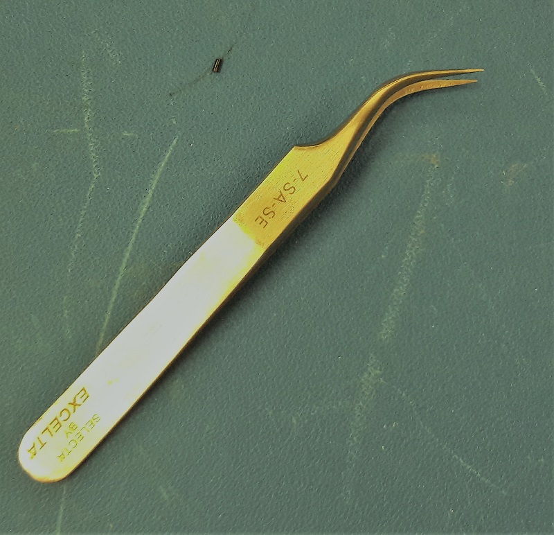
Fig. 4: If you work with small electrical elements, invest in a pair of tweezers that makes your job easier.
It takes long hours of practice to reach a point of being able to confidently and neatly place a part on a board without damaging it. As you start the process, it is very helpful to keep your goal in mind. Pick your practice board. Put it under the microscope and examine the pad areas where you are planning to solder your part.
Are they clean? If not, you have some work to do. Apply a droplet of flux on that pad. Afterward, you will need an iron in one hand and a stream of solder wick in the other. Place the stream on the not-very-clean pad and come closer with the iron tip. Every now and then, you should look from outside the microscope just to make sure that you are not driving the iron tip toward yourself or your arms. The tip is 800°F (I sometimes wonder how the tip itself does not melt).
Now place the iron tip softly on the solder wick and press it toward the board. Wait for that moment of victory when the soldering melts and moves toward the heat source. (This is why we applied the flux. Flux makes the solder move toward what’s hotter.) Then grab the wick, smoothly collecting the unwanted soldering. Is it clean? If not, repeat the process. And do not be shy to repeat this a couple of times. A good practice is to stick some soldering onto a random pad and clean it over and over just to get comfortable with the cleaning process. Now that the pad is clean, we need to get it ready for soldering the part to it. To do so, we will apply some soldering. Yes, after we have just removed all the soldering on the pad, we will apply fresh soldering. (I understand that there are different schools of thought here. I prefer to go with cleaning and applying fresh solder rather than reusing. I believe it’s tidier that way.)
Now, let’s get started and apply some flux to the pad. Hold the iron in your preferred hand and the solder wire in the other hand. Adjust your hands to be as close as possible to the pad you are working with. Look into the microscope. Bring the iron and solder wire very close to the pad.
In a split second, you will see the wire forming some soldering on the pad. Move your iron and solder wire away once this happens. This is not that easy. You will have to repeat this technique nearly a hundred times before you feel comfortable doing it — just as it might take you a hundred attempts to begin to master the fundamentals of a guitar chord.
Now, using your tweezers, grab the part that you want to solder. Hold the tweezers in a way that feels comfortable. You will soon be trying to push the part about 0.01 mm of distance. Bring the part very close to the pad where you just applied some fresh solder. Move the iron with your other hand and let the tip touch the solder on the pad. Once the solder has melted, quickly but firmly move the part far enough away that it contacts the solder that you applied. Yes, this requires a lot of practice to master as well.
Now, we still need to solder the other side of the part to the board. This is done by quickly heating one side of the part with the presence of solder wire. In a split second once again, if there was enough flux, the soldering will make contact between the part and the pad. Well done! Or more likely, let’s do that again and try to make it look/work better.
There is so much more to do with a PCB and a few parts. Attaching a new part to a pad is definitely the first step. But along the way, you may need to remove the part and attach another one. It also takes skill to remove that part without damaging it and attaching it again (yes, I have seen it work).
Partnered Content: Learn why signal chain expertise is mission-critical for the DOD
On a more complicated level, there is the soldering of an IC package. For example, my soldering mentor told me how an R&D project used the excess soldering to improve matching network characteristics.
The lesson that I’ve learned about soldering is that there is so much to learn. Every time you think that you have mastered a soldering technique, a new challenge arises. That is not something to worry about. We engineers enjoy being challenged.
Unlike most of the other engineering tasks that you might encounter in your job, the best approach to learning how to solder is by doing and not by reading books and articles about it. While these can be helpful resources to expand on some technical issues or gain insight from experts, the best way to learn soldering is to do it yourself!
It’s also helpful to ask others in person for their advice and insights. Tap the expertise of a technician in your company’s lab who can solder a few chips in an hour. They carry the art within their fingers. And after a few simple questions, they will divulge many helpful tips. They did not learn these tips through reading. They learned them by trial and error.
In closing, another smart engineer at my company advised, “You have got to own your own destiny.” In other words, when you take charge of more jobs and different phases of your project, your feeling of ownership grows. The project becomes your own creation.
To put it another way, as an electrical engineer, it will help you immensely to learn the art of soldering. This essential skill will not only make it faster for you to pinpoint an open solder the next time that you suspect one, it will also make your communication with the soldering specialist a lot easier. You now speak their language, and you understand their unworldly capabilities.
Asem Elshimi is an RFIC design engineer for IoT wireless solutions at Silicon Labs. He joined Silicon Labs in July 2018. Elshimi specializes in the areas of RF circuit design and electromagnetic structure design. He holds an M.S. in Electrical and Computer Engineering from the University of California, Davis.
Advertisement
Learn more about Electronic Products Magazine


