By Junko Yoshida, global co-editor-in-chief, AspenCore Media, and chief international correspondent, EE Times
In a flash sale that was reportedly over in 10 seconds, Huawei launched in China today its brand new P30 and P30 Pro smartphones.
Along with the launch, different technology outfits scrambled to break apart the new handsets so that they could be the first to post teardown reports.
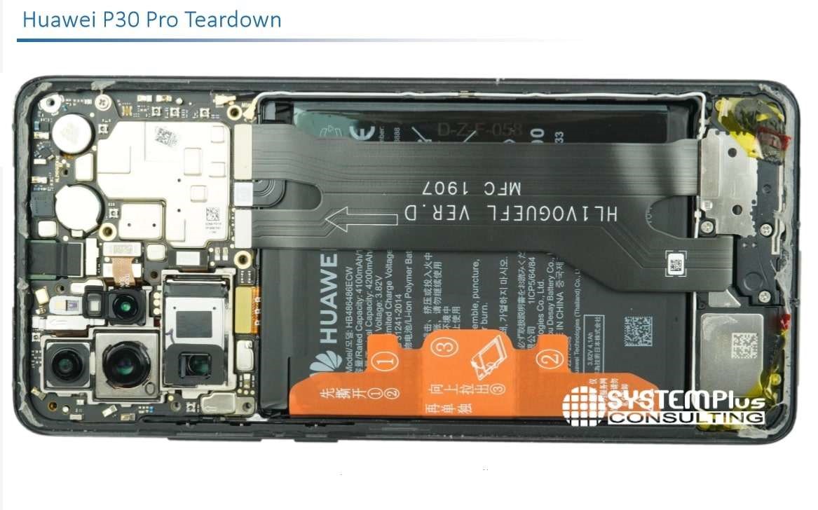
Image: System Plus
EE Times tapped the technical expertise of System Plus Consulting (Nante, France), Yole Développement’s partner company. We asked the analysts to share their initial observations and reveal any surprises that they encountered.
Stéphane Elisabeth, costing analyst expert at System Plus Consulting, told us that the focus of their P30 Pro teardown was squarely on quad cameras — including a periscope camera capable of 10× zoom. The periscope camera claims no loss in image quality, while the smartphone does not need to use a long-barrel telescopic lens.
But as the team dissected the P30 Pro, a few surprises popped up, Elisabeth told us.
Three-stack PCB
First, Huawei is now using a three-stack PCB configuration in P30 Pro. While Apple was the first smartphone vendor to do three-layer PCB in the iPhone X and Samsung followed suit, the System Plus crew didn’t expect Huawei to catch up so soon.
It turns out that Huawei has used substrate-like PCB (SLB) assembly from Taiwan-based PCB supplier Unimicron. Apple’s iPhone X three-stack PCB was assembled by Austria-based AT&S.
While both the P30 Pro and iPhone X use similar PCB architecture in three layers, the way in which they use the stacks is different.
In the P30 Pro, the bottom layer embeds Huawei’s chip division HiSilicon-developed Kirin applications processor, power management ICs, and passives. All RF components occupy the top layer. In between, a mid-frame PCB connects the two and serves as an isolation layer, Elisabeth explained.
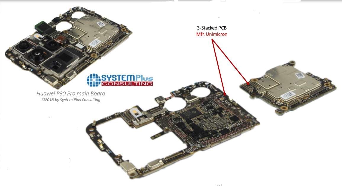
The Huawei P30 Pro three-stack PCB. The main board uses three pieces of PCB manufactured and assembled by Unimicron. The first PCB has the application processor and the power management ICs and passives. The second is a single-sided PCB with all of the RF components. Between these two pieces, a mid-frame PCB is used to make the connections. (Image: System Plus)
In contrast, Apple, in its iPhone X, placed memory on the top layer and an application processor in the middle layer. The third layer, providing thermal dissipation, was left blank.
The advance of stacked PCB architecture is important, System Plus’s Elisabeth explained, because it enables the development of “a substrate-like PCB with very thin copper lines.” The end results are “a powerful PCB with no loss in power and latency, while saving space,” he added.
Four cameras
Separating Huawei P30 Pro, more than anything else, is its use of quad cameras. The new smartphone literally has four cameras. They include a main camera, plus cameras for wide-angle, time-of-flight (ToF), and periscope view. All four use Sony CMOS image sensors. “It’s a full design win for Sony,” said Elisabeth.
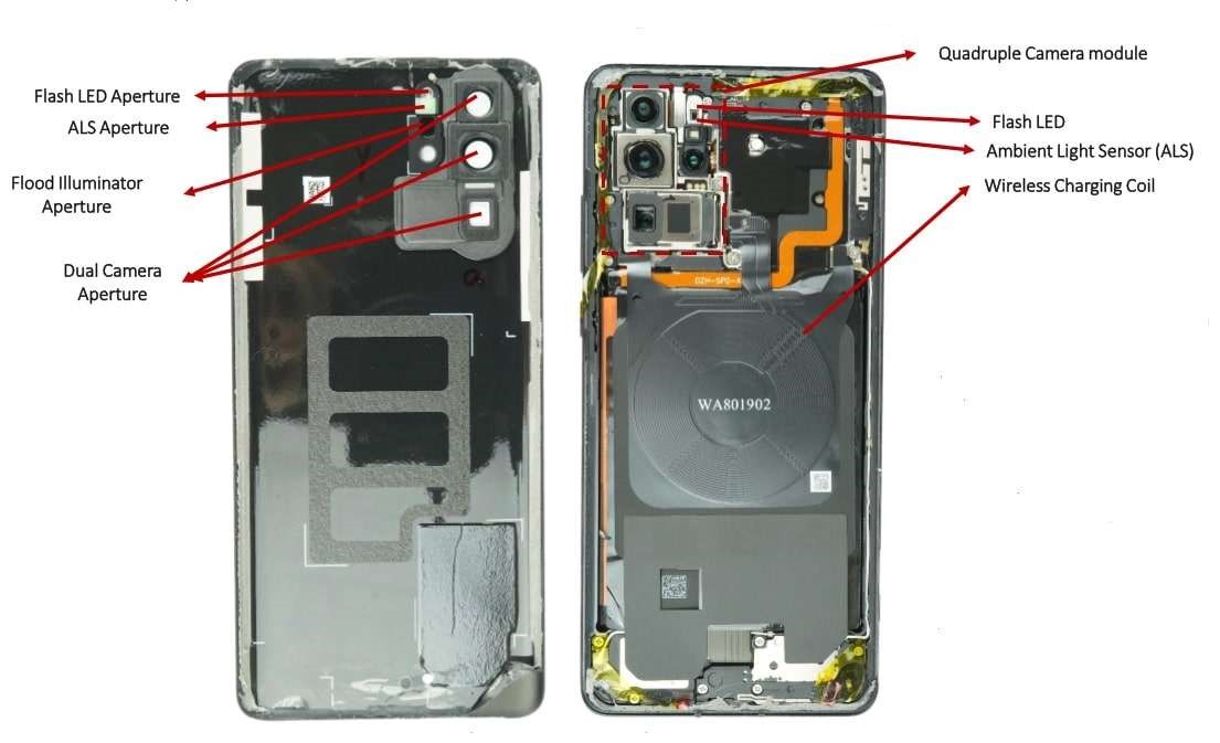
The Huawei P30 Pro opened view. The Quad Camera module uses several different architectures. A periscope camera module is used to enable 10× zoom, a ToF camera module coupled with a flood illuminator is used to enable AR functionality, and a dual camera with a wide angle and a main camera. (Image: System Plus)
A dual-camera module uses a filter consisting of RYYB [Red, Yellow, Yellow, Blue] instead of the usual RBG. While the main camera’s image sensor supplies RGB signals, the RYYB filter helps to bring in more light, according to Elisabeth.
Another item to note with P30 Pro is the addition of a Sony ToF camera. While Huawei isn’t the first to use Sony’s ToF camera (China’s Oppo is already using it), Huawei uses it not only for augmented reality (AR) applications but also for “auto-focus,” Elisabeth noted.
By processing signals from all three cameras, the ToF camera helps map out a scene and allow a user to focus on a specific object. “This is the first time a ToF camera is being used for auto-focus,” Elisabeth stressed.
For the complete teardown, visit EE Times.
Advertisement
Learn more about Electronic Products Magazine


