By Majeed Ahmad, contributing writer
Lattice Semiconductor has released new reference designs that are built around its CrossLink FPGA and are targeted at video-bridging applications. The SubLVDS to MIPI CSI-2 image sensor bridge reference design allows developers to connect application processors with image sensors used in machine vision applications for industrial environments.
Many industrial device OEMs want to implement application processors in the existing machine vision-capable products. However, many industrial machine-vision applications use image sensors with a SubLVDS interface, which is incompatible with the MIPI CSI-2 D-PHY interface used on today’s application processors.
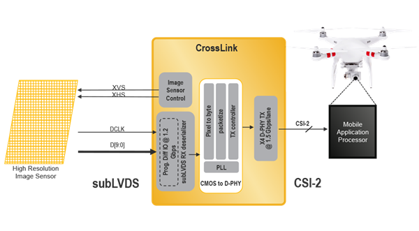
The reference design enables engineers to quickly and easily create a bridging solution to connect an application processor using the MIPI CSI-2 interface with a SubLVDS image sensor. It’s a simple workaround that addresses the legacy interface compatibility issues.
Key features include:
- 4-, 6-, 8-, or 10-lane SubLVDS input to 1-, 2-, or 4-lane MIPI CSI-2 output
- Up to 1.2 Gbits/s bandwidth per input lane
- Up to 1.5 Gbits/s bandwidth per output lane
- Dynamic parameter setting via I2C
- Optional support for image cropping
The reference design is free and can demonstrate the use of Lattice’s CrossLink modular IPs, including the Pixel-to-Byte converter IP, SubLVDS image sensor receiver, and a CSI-2/DSI D-PHY transmitter. It comes with an easy-to-use GUI-based FPGA design and verification software environment: Diamond design software .
Advertisement
Learn more about Electronic Products Magazine


