By Maurizio Di Paolo Emilio, editor, Power Electronics News
Power management theory has led to the development of integrated circuits that are specialized in carrying out regulation and conversion functions. These power management ICs (PMICs) can be part of the microcontroller die or standalone components housed in packages compatible with the latest generation of integrated circuits.
Devices equipped with PMICs tend to be smarter and more efficient, as they regulate the flow of energy from inside and outside the device. A key factor contributing to the increased use of PMICs is the growing demand for energy-saving products. They are used in consumer electronics, automotive, industry, telecommunications, and networks.
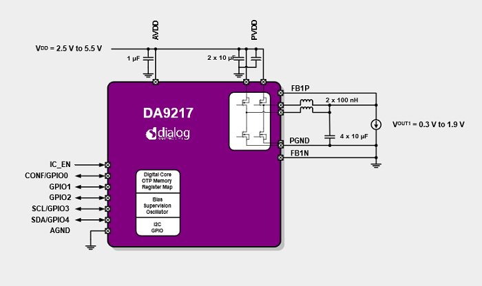
One such product is a new family of buck converters from Dialog Semiconductor, consisting of the DA9217, DA9220, DA9121, and DA9122, which represents the company’s first sub-PMIC family with a 4-MHz switching frequency that reduces the size of the inductor to allow the use of smaller external components. The devices are suited for multi-core processors based on ARM Cortex, and high-performance SoCs, FPGAs, and GPUs, which allow developers to adapt a power solution from 6 to 10 amps (A) in next-generation devices (Fig. 1 ).

Fig. 1: An application circuit of the DA9217.
“Target markets for the new product family include smartphones, digital still cameras, solid state drives, hard disk drives, notebook PCs, Wi-Fi modules, optical transceiver modules. In these applications, the new sub-PMICs are typically powering CPU cores in the system’s application processor or supplying power for system memory,” said Faisal Ahmad, director of marketing, power management at Dialog Semiconductor.
The devices ensure greater efficiency by simplifying the complex system sequencing with easy digital programming. The devices can support a single output up to 6/10 A or dual outputs up to 3/5 A per output, making it well-suited for the latest 7-nm based SoCs.
The sub-PMICs can operate with a single-cell lithium-ion battery, and the I2C interface allows dynamic voltage control to optimize energy savings and performance. The functions of fault protection also provide protection against overvoltage, overcurrent, and thermal shutdown.
“Dialog’s new product family offers autonomous power modes including PFM mode, phase shedding mode, and full power PWM mode that optimizes system efficiency based on output load profile. An advanced technique would involve dynamically changing voltage depending on CPU loading ahead of the actual operation in the CPU,” said Ahmad.
“For example, if a user on a mobile device loads a game with advanced graphics, the CPU requests the voltage that optimizes the performance and power consumption based on the cores in the CPU to be active to run that application,” he continued.
The thermal behavior of integrated circuits is by far essential to avoid overheating that can cause malfunctions. Designers need to know the thermal behavior of an IC, particularly for PMICs used in automotive applications. Finding an optimized solution requires a good understanding of predicting the operating temperatures of system power components and how the heat generated by these components spreads to nearby devices. Furthermore, as reliability requirements become increasingly stringent, there is a growing concern about the effect of temperature change on package integrity.
“Anytime you approach 10-A total output current in a small form factor, thermal management becomes very important. The WLCSP package used in this product family provides very good thermal performance. This also provides layout recommendations to optimize the efficiency and thermals,” said Ahmad.
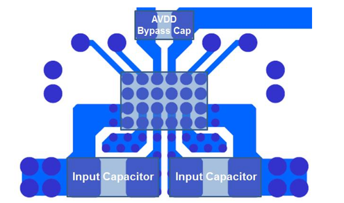
“The WLCSP package layout and recommended board layout emphasize placing decoupling capacitors very close to the device with short but wide traces for the input power and ground routing to minimize losses. The inclusion of added vias from the input and ground planes to inner layers helps to improve thermal performance by drawing heat from the device into the PCB (Fig. 2 ),” Ahmad added.

Fig. 2: Recommended input capacitor placement and routing.
Most consumer electronic products are based on PMICs. As these consumer devices evolve, designers face the constant challenge of trying to reduce the board's footprint and reduce energy consumption.
“The key technical challenges in power management design are solution size and efficiency. For further reduction in solution size, we are looking at switching at frequencies >10 MHz to further reduce the size of the output inductor and capacitors. Improving efficiency provides the benefits of simplifying thermal design and extending battery life in mobile applications,” said Ahmad. “Dialog is developing improved device technology that provides more efficient switching as well as new switch-mode architectures that provide inherent power loss reductions.”
PMICs help to reduce the size of the final product, increase the overall efficiency of the system while reducing heat dissipation. As the industrial sector evolves and creates new complex and connected industrial systems, power management must also meet the new design challenges. Form factor, design, and energy efficiency are essential to realizing new devices, but they also must be attractive and easy to use, offering new ways to improve our productivity, health, and lifestyle.
Advertisement
Learn more about Electronic Products Magazine


