By Junko Yoshida, global co-editor-in-chief, AspenCore Media, chief international correspondent, EE Times
Gigahertz is where no microcontroller vendor has gone before, but FinFET is even deeper in outer space for the MCU sector. MCU powerhouse NXP, determined to outpace its peers, has crashed through the GHz barrier and might be on its way to a FinFET MCU.
It was exactly a year ago when Geoff Lees, senior vice president of microcontrollers, NXP Semiconductors, tipped NXP’s plan to launch a GHz MCU in 2019 . Keeping his word, Lees this week unveiled i.MX RT1170. NXP claims that the new family of “crossover MCUs that breaks the gigahertz barrier” will accelerate advanced machine learning (ML) applications at the edge.
Instead of the growing number custom AI accelerators — often tailored for specific AI applications — populating the market today, Lees is confident that NXP now has what OEMs want.
During the interview, Lees also hinted that NXP is preparing a FinFET MCU for 2020 launch. For NXP, the MCU business is all about a broader, scalable portfolio. The company revealed plans to cover everything from crossover MCUs in 40nm (starting at $1), GHz MCUs with low-leakage in FD-SOI, and in the future, at an appropriate time, performance optimized MCUs in FinFETs.
‘Crossover MCU’
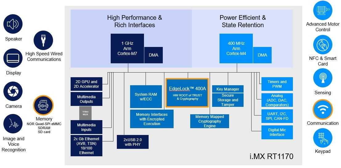
NXP’s new GHz MCU integrates high-performance Cortex-M7 with power-efficient Cortex-M4. The new MCU can be used as a standalone microcontroller or it can be dropped inside an application processor, Lees explained.
The i.MX RT1170 dual-core system is a key advantage offered in NXP’s new GHz MCU. The dual-core system pairs a high-performance core and a power-efficient core with independent domains of operation. This enables developers to run applications in parallel or reduce power consumption by turning off individual cores as necessary, NXP explained. For example, the energy-efficient Cortex-M4 core can be dedicated to time-critical control applications, such as sensor hub and motor control, while the main core runs more complex applications.

i.MX RT1170 system overview. (Image: NXP)
NXP is “essentially giving you application processor functionality and performance, with power and performance-optimized cores in an MCU,” observed Jim McGregor, principal analyst at Tirias Research.
But NXP’s move to blur the line between MCUs and apps processors under the “crossover” moniker might take some time for the industry to embrace.
Speaking of i.MX RT1170, Tom Halfhill, a senior analyst at The Linley Group, observed, “It appears to be an unusually fast processor of its type with lots of on-chip SRAM, I/O interfaces, and peripherals, including ADC, DAC, and Ethernet with industrial TSN… Some models will be rated for industrial and automotive temperatures. It has strong security features, and the dual cores can run in isolation from each other but can also share all the peripherals and I/O.”
However, Halfhill added: “We're not particularly fond of the ‘crossover MCU’ terminology. These devices aren't MCUs in the traditional sense because they lack internal flash memory. But flash is difficult to implement in IC technologies smaller than 40nm, so these devices must depart from the traditional definition in order to deliver higher performance.”
Halfhill summed it up: “The i.MX 1170 employs high-performance 28nm FD-SOI technology, so it combines the features of an MCU (except flash) with the performance of a relatively fast embedded processor.”
Focus on power efficiency
The silver bullet for the i.MX1170 is its low power. In developing crossover MCUs, NXP has kept its eye on maintaining power efficiency.
Specifically, the i.MX RT1170, built in 28-nm FD-SOI, has a typical active power consumption of
Further, the i.MX RT1170 (28-nm FD-SOI) has several standby power modes: low-power idle is
Run multiple ML apps concurrently
By using the same underlying hardware architecture as that of an application processor, NXP renders crossover MCUs more flexible and scalable, said Lees. Rather than developing a custom accelerator for different AI application, “We are starting with an application processor architecture and maintaining its scalable fabric, thus making [crossover MCU] far more flexible than flash MCU,” said Lees.
By allowing hardware/software platform reuse across different applications, NXP claims its crossover MCUs will be “very attractive for OEMs.”
Notably, the dual-core system embodied in the i.MX1170 can run Machine Learning (ML) applications in parallel, such as face recognition with natural language processing to create human-like user interactivity.
Now that the i.MX RT1170 has enough total horsepower (from M7 at 1 GHz + M4 at 400 MHz), the new GHz MCU can run “multiple ML applications, for example, face recognition, local and far-field voice controls, concurrently,” said Lees.
Indeed, OEMs can keep the hardware platform the same, but “bolt-on” one or more capabilities from a list that encompasses face, voice, far-field voice, gesture, tone, anomaly detection, and graphics depending on the application, the company explained.
But, really, who needs multiple ML apps at the same time?
Smart home IoT devices are evolving to combine face recognition with voice and gesture recognition to create a more human-like interaction with “things,” according to NXP. “We also see ‘expression’ and ‘tone’ recognition being added so that voice assistant devices can better interpret human emotions.” Further, even in the industrial settings, there are instances in which face with voice recognition could be used to control access to secure areas and machines, NXP added. “Voice plus gesture could then be used by the operators to interact more easily with controls.”
What’s inside?
There are a number of features embedded inside the i.MX RT1170 MCU.
In addition to a dual-core architecture with the Arm Cortex-M7 core running up to 1 GHz and Cortex-M4 running up to 400 MHz, these include: 2D vector graphics core, NXP’s pixel processing pipeline (PxP) 2D graphics accelerator, and NXP’s advanced embedded security technology.
Its architecture is designed to deliver a 12 ns interrupt response time, 6468 CoreMark score and 2974 DMIPS while executing from on-chip memory, according to NXP. The new MCU crossover integrates up to 2 MB of on-chip SRAM, including 512 KB configurable as tightly-coupled memory (TCM) with error code correction (ECC) for Cortex-M7 use, and 256 KB of TCM with ECC for Cortex-M4 use.
The TCM is designed to provide low-latency memory to the processor without unpredictability, according to Arm.
As of now, NXP’s GHz MCU is in a league of its own. Whether competitors will seek a similar “crossover” option remains to be seen. McGregor said, “The other likely players would be other MCU vendors like STMicroelectronics, Renesas, and Microchip. We will have to wait and see if they want to push MCUs into this ‘crossover’ category.”
Lees believes firmly in a growing demand for application processors at MCU-like ultra-low power. Cloud companies such as Microsoft, Google and Amazon are prompting NXP to heed this trend, said Lees. “It’s taking a little long for others to catch up [with crossover MCUs], but we believe our MCU competitors will soon follow suit.” He added that some Chinese fabless companies are also curious.

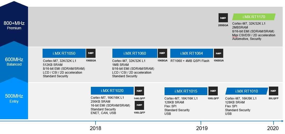
i.MX RT series portfolio. (Image: NXP)
First FinFET MCU to debut in 2020
In discussing the never-ending quest for lower-power, higher-performance MCUs, Lees hinted: “Don’t be surprised to see the first FinFET MCU from us a year from now.”
NXP explained that its goal is to provide customers a “scalable portfolio with performance, power, and cost optimized products so that they can choose the MCU that best fits their application need.” This means, aside from crossover MCUs in 40nm and GHz MCUs with low-leakage in FD-SOI, NXP is working on MCUs in FinFETs focused on performance improvement.
Does this mean that at some point, NXP will stop using FD-SOI?
Not at all, said NXP. The company insisted that it will not stop 28nm FD-SOI based RT MCUs.
Consider the current GHz MCU. On one hand, “What made the low active power of GHz MCU possible is specific SoC management of the core-complex and peripherals in run mode and integration of DC-DC converter into the chip itself,” according to NXP. On the other, “Low standby power is from combination of FD-SOI technology and SoC architecture.”
The reasons NXP pushes 28nm FD-SOI based RT MCUs are manifold.
NXP likes its performance-power tunability and cost effectiveness. “FD-SOI is unique in its ability to modulate power-performance with body biasing — forward bias for higher performance and reverse bias for lower off-state leakage, so in our future 28nm FD-SOI MCUs, we will dynamically ‘tune’ power-performance on a die-by-die basis – that level of flexibility is not possible with 28nm high-K metal gate processes,” the company noted.
Further, ultra-low leakage with long battery life is particularly important for “edge” applications, NXP said. “We have reduced 28nm FD-SOI SRAM leakage (a big component of standby power when SRAM needs to be retained for fast wakeup) to 10x improvement over 28nm high-K metal gate process.”
Indeed, one key advantage for NXP’s MCUs is its large portfolio.
McGregor pointed out, “NXP has more MCU/MPU product SKUs than any other vendor and they also provide reference designs and tools for all their products.” He explained, “The benefit of having more products that push the boundaries of traditional product families is that you can get something off-the-shelf with full support rather than designing a custom SoC.”
He observed, “Many companies are going down the custom SoC route because it is easier than ever to do so, but it is still expensive and somewhat risky. In many applications, you are better off designing around standard products and allowing for room to grow in performance either through additional products in the family or in the products you choose.”
Speaking of NXP’s GHz MCU, the Linley Group’s Halfhill observed, “It's not strictly an AI processor or accelerator, so it won't compete with chips specially designed for that purpose. But at 1 GHz, the main CPU can handle some ‘AI’ tasks without a separate accelerator. It will be useful in some applications that need rudimentary voice or face recognition.”
But NXP’s Lees is far more ambitious. Armed with the company’s eIQ, a collection of libraries and development tools for building ML apps using NXP MCUs and app processors, NXP envisions much more room to grow for its MCUs in the AI space.
The company’s plan for the first FinFET MCU in 2020 should also help. The only difference is that NXP is determined not to give short shrift to the power efficiency inherent in MCUs. As vendors look ahead for MCUs or apps processors emerging two years from now, the first thing they consider is how many teraflops they can achieve on the new processors, said Rees. But for NXP, according to Rees, it’s is not all about teraflops. “We think about what other [AI] apps we can run with today’s $2 face recognition MCU — two years from now.”
Pricing and availability
The i.MX RT1170 will start at $4.48 resale for quantities of 10k, according to NXP. A full-featured super set will be in the mid-$5 range.
Asked about availability, NXP said it is “currently working with several lead customers, providing them with samples and evaluation kits.” In parallel, NXP is doing internal software development and working with ecosystem partners to develop software libraries (especially for 2D vector graphics, TSN, and ML applications). NXP hopes its customers can use the full power of the i.MX RT1170 when it becomes generally available in the second half of 2020.
The article originally published on sister publication EE Times.
Advertisement
Learn more about Electronic Products Magazine


