By Soufiane Bendaoud, precision amplifiers, Texas Instruments
With high-accuracy designs comes a set of challenges that ultimately dictate component selection. Designers are often faced with the dilemma of trying to achieve the best of two worlds. They must attain their design goals by carefully selecting devices, but these devices cannot always meet all of the requirements.
For example, when designing with higher-resolution converters, you need to select the analog front end (operational amplifier [op amp], instrumentation amplifier [INA], or programmable gain amplifier [PGA]) based on the output impedance of the sensor with which it interfaces in order to avoid gain errors caused by loading effects. But you must also consider the sampling rate of the converter as well as the settling time, as these two parameters will affect your choice of op amp.
A low-power unity-gain-stable op amp will lack the required bandwidth and slew rate, resulting in erroneous readings of settling time. A 16- or 18-bit analog-to-digital converter (ADC) needs a low-noise analog front end in order to maintain signal integrity.
Table 1 lists common sensor types with the corresponding choice of amplifier based on the process technology and expected magnitude of input bias current (Ib).
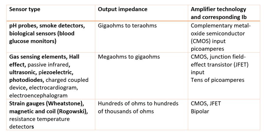
Table 1: Common sensor types
What does sensor type have to do with Ib?
The reason I suggested very low-input-bias-current op amps for very high-impedance sensors has to do with the noise and offset errors caused by the interaction of Ib with the input impedance (source resistance). When interfacing with gigaohm to teraohm source impedances, you should use a very low-input-bias-current type of amplifier such as a CMOS input.
Even then, remember that very low Ib will be a great advantage at room temperature only. As the temperature increases, the input bias will increase exponentially, doubling every 10°C of increase in temperature. A 1-pA op amp at 25°C will see about 1 nA at 125°C.
Another concern comes from the shot noise equation, expressed as Equation 1:

where q is the charge of an electron (1.6 × 10⁻¹⁹ C) and Ib is the input bias current.
Needless to say, with a source impedance in the gigaohm range, current noise is a major concern. For even larger impedances, ultra-low-input-bias-current op amps such as the Texas Instruments (TI) LMP7721 have a clear advantage.
Input current noise is only part of the story. In applications with slow-moving signals (such as temperature monitoring) or those with narrow frequency bands (such as medical instrumentation and audio), the 1/f component will dominate total noise. In such cases, a good choice would be a JFET, which has a much lower Ib than its bipolar junction transistor counterpart and, at the same time, a lower 1/f noise corner compared to CMOS technology.
Does voltage noise matter less with a high source impedance?
Just like everything else in electronic design, the answer is that it depends. If the source impedance is very high, it is likely that current noise will dominate. However, a good practice is to account for all sources of noise, even for an ultra-low-input-bias-current op amp.
Remember that voltage noise is inversely proportional to current, whether that’s the collector current in bipolar process technology or the drain current in CMOS. For the voltage noise to be low, you must supply a high level of current (quiescent current) into the op amp — which, in turn, will cause an increase in the bandwidth, being that the gain bandwidth product (GBW) is expressed as Equation 2:

where gm is Ic/VT in bipolar technology and in CMOS.
Because the noise is integrated over the bandwidth, low-noise amplifiers (instrumentation, programmable, differential) are only advantageous if their bandwidth is limited.
The impact of front-end noise on the rest of the circuit
Because noise sources are usually uncorrelated, you can add them in a root sum square (RSS) fashion. The higher the noise of the analog front-end portion, the more it will dominate the total noise (root mean square [rms]). A noise source of 5 nV added to another source that’s 3 nV yields 5.8 nV (rms). Clearly, the larger of the two dominates.
To get a better feel, let’s compute the total signal-to-noise ratio (SNR), ignoring for simplicity the signal-to-noise and distortion ratio. The SNR of the converter is usually given in the data sheet in decibels and can be expressed as Equation 3:

where n is the resolution or number of bits.
To compute the SNR of the op amp, PGA, or INA, first compute the total noise in RSS. See Fig. 1 .
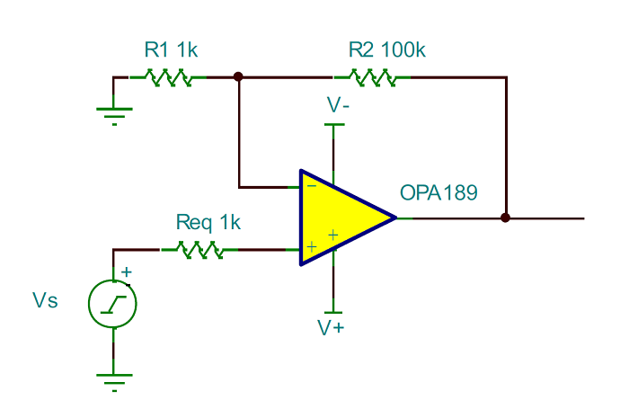
Fig. 1: OPA189 rms noise and SNR
Rather than using the gain setting and feedback resistors individually, for noise calculation, you can use the equivalent parallel combination represented by the Req resistor. As such, Req = 990 Ω, which for all practical purposes is close to 1 kΩ.
The thermal noise of the external resistors is expressed as Equation 4:

where k is the Boltzmann constant and is equal to 1.38 × 10⁻²³ m2 kg s–2 K–1 and T = 298K.
A quick shortcut for thermal noise is to use Equation 5:

where R is the resistor value in kiloohms. A 1-kΩ resistor has

while 100 kΩ generates

at a room temperature of 25°C or 298K.
The TI OPA189 has a voltage noise density (en ) of

and a current noise density of

at 1 kHz. The contribution of the current noise is eni = 165 x 10–15 × 1 × 103 = 165 × 1012 .
Equation 6 expresses the total noise (en_total ) as:

which is

To calculate the rms noise at the output, you first need the closed-loop bandwidth, fc , which is defined as Equation 7:

where GBP is the gain bandwidth product and NG is the noise gain. Plugging in values, Equation 7 results in (14e6 /101) = 139 kHz.
The total rms noise is then expressed as Equation 8:

where NG is the noise gain and NBW is the noise bandwidth, which is defined as: fc = 1.57 × fc = 218 kHz. Plugging in values, Equation 8 results in

where the simulated rms noise showed 300 µV.
Equation 9 calculates the SNR of the op amp:

where VFSR is 2.5 V and Erms is 310 µV from the previous calculation. The calculation yields 71.3 dB versus 70.6 dB from the simulation.
Figs. 2 and 3 show simulations of the total noise (rms) and SNR, respectively.
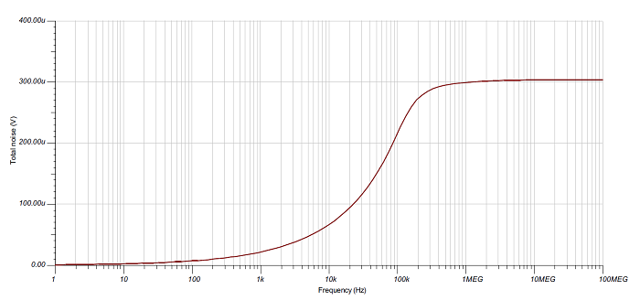
Fig. 2: OPA189 rms noise
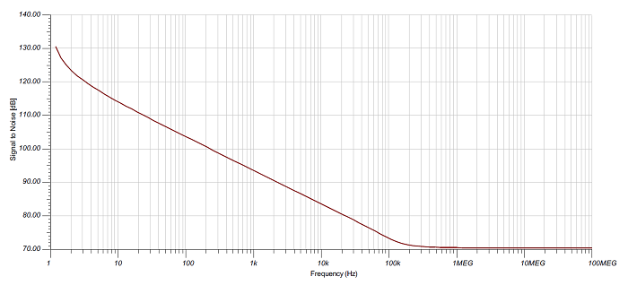
Fig. 3: OPA189 SNR plot
If you were using the TI ADS8922B 16-bit ADC with a typical SNR of 92 dB and a precision voltage reference like the TI REF5025, the low value of the op amp’s SNR would degrade the overall performance. A quick noise simulation of the REF5025 reveals the SNR to be about 85 dB (see Fig. 4 ). You can calculate the total SNR for the system (op amp, ADC, and voltage reference) using Equation 10:

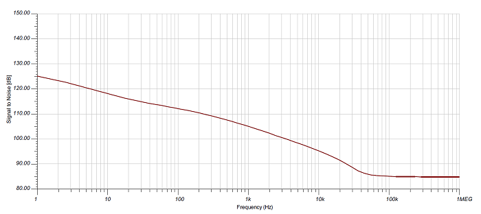
Fig. 4: REF5025 SNR plot
It is possible to improve the amplifier noise by placing a capacitor in the feedback loop. One question you might ask is where to set the cutoff frequency.
One of the advantages of simulating the noise (when modeled accurately) is that the plot of total integrated rms noise helps you quickly determine the filter cutoff frequency based on what value of noise is acceptable to you.
For example, if you want to reduce the OPA189 output rms noise to 50 µV, set your filter cutoff frequency at fc = 6 kHz/1.57 (you need to divide 6 kHz by 1.57 to account for the difference between signal bandwidth versus noise bandwidth in the case of first-order bandwidth rolloff).
In order to lower the noise bandwidth with a capacitor across the feedback resistor, calculate the capacitor value as:

which yields 416 pF.
With the capacitor in place, the total rms noise is 50 µV. The op amp SNR improves by 15 dB to 86 dB, as shown in Figs. 5 and 6 . Using Equation 10, the total SNR is now 82 dB.
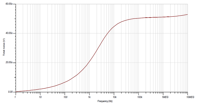
Fig. 5: OPA189 rms noise with filter
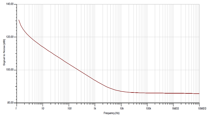
Fig. 6: OPA189 SNR with filter
There are other parameters to consider when designing with high-resolution converters; more than what I covered in this article. Carefully looking at the PGAs, op amps, INAs, and other analog front-end components and their process technologies can help you select a suitable device more confidently.
Although bipolar-input op amps tend to exhibit a much higher input bias current and current noise, super-beta technology reduces it quite a bit. As an example, the OPA202 has a maximum input bias current of 2 nA and a current noise of 76 fA.
Be cautious when looking at op amps with input bias current cancellation techniques. The current noise calculation will increase by about 41% above what it should be for an uncancelled value of Ib. A quick way to determine whether the amplifier you’re considering uses a cancellation scheme is to look at the specification table in the data sheet. If you see a ± sign, the amplifier has a cancellation scheme.
Advertisement
Learn more about Electronic Products MagazineTexas Instruments


