Advanced IC packaging is a prominent technology highlight of the “More than Moore” arena. At a time when chip scaling is becoming more difficult and expensive at each node, engineers are putting multiple chips in advanced packages as an alternative to chip scaling.
However, while advanced IC packaging is evolving rapidly, design engineers and engineering managers must keep pace with this crucial technology. For a start, it’s important to understand the basic terms that keep coming in advanced IC packaging content.
![]() Editor’s Note: This article is part of an AspenCore Special Project, a collection of interrelated articles that explores advanced IC packaging. See all the articles in this Special Project below.
Editor’s Note: This article is part of an AspenCore Special Project, a collection of interrelated articles that explores advanced IC packaging. See all the articles in this Special Project below.
Here is a brief synopsis of the 10 most common terms used in next-generation IC packaging techniques:
2.5D packaging
In 2.5D packages, dies are stacked or placed side by side on top of an interposer based on through-silicon vias (TSVs). The base, an interposer, provides connectivity between the chips. An incremental step from traditional 2D IC packaging technology, 2.5D packages enable finer lines and spaces.
2.5D packages are commonly used in high-end ASICs, FPGAs, GPUs, and memory cubes. In 2008, Xilinx partitioned its large FPGA into four smaller, higher-yielding chips and connected those chips on a silicon interposer. That led to the birth of 2.5D packaging, which eventually became popular for high bandwidth memory (HBM) processor integration.
Here is a schematic of a 2.5D package. Image: Research Gate
3D packaging
In 3D IC packages, logic dies are stacked on each other or memory dies instead of creating a large system-on-chip (SoC), and dies are connected using an active interposer. Unlike 2.5D IC packages that stack components on an interposer through conductive bumps or TSVs, a 3D IC package employs multiple layers of silicon wafers stalked together along with components using TSVs.
TSV is a key enabling technology in both 2.5D and 3D IC packaging technology. The semiconductor industry has been shipping DRAM chips in 3D IC packages using the HBM technique.
This 3D package cross-section shows the use of Cu TSVs for vertical interconnection between Si chips. Image: Research Gate
Chiplet
A menu of modular chips in a library that can be integrated into a package using die-to-die interconnect, chiplets are another form of 3D IC packaging that enable heterogeneous integration of CMOS devices with non-CMOS devices. In other words, they are smaller SoCs, or chiplets, instead of one big SoC in a package.
The idea is to break a large SoC into smaller chiplets for improved yield and lower cost than a monolithic die. Chiplets allow designers to leverage various IPs without considerations of which node or technology they are manufactured on; they can be built on a variety of materials, including silicon, glass, and laminate.
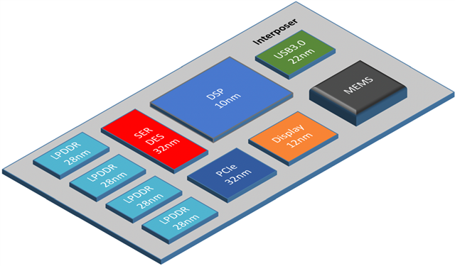
A chiplet-based system is made of multiple chiplets on an interposer. Image: Cadence Design Systems
Fan out
Fan-out packages, in which connections are fanned out of the chip surface to facilitate more external I/Os, use an epoxy mold compound to fully embed the dies, so they don’t require process flows such as wafer bumping, fluxing, flip-chip assembly, cleaning, underfill dispensing, and curing. That, in turn, eliminates the need for an interposer and makes the implementation of heterogeneous integration simpler.
Fan-out technology provides a small form-factor package with more I/Os than other package types. It thrust to technology stardom in 2016 when it enabled Apple to integrate its 16-nm application processor with mobile DRAM in one package inside iPhone 7 using TSMC’s packaging technology.
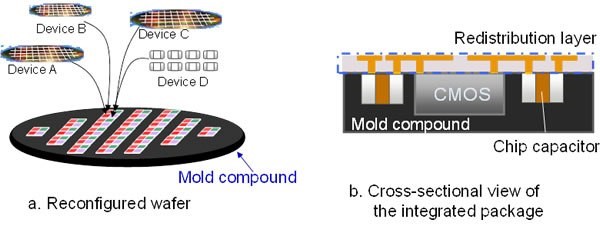
Fan-out wafer-level packaging (FOWLP)
An improvement over wafer-level packaging (WLP), the FOWLP technique has been developed to provide more external contacts with silicon die. It embeds chips inside the epoxy molding compound and then fabricates high-density redistribution layers (RDLs) and solder balls on the wafer surface to form a reconstituted wafer.
Typically, it first dices the front-end processed wafer into individual die, and then dies are spaced apart on a carrier structure and the gaps are filled in to form a reconstituted wafer. FOWLP provides a larger number of connections between the package and the application board. Moreover, the substrate is essentially bigger than the die, so the die spacing is more relaxed.
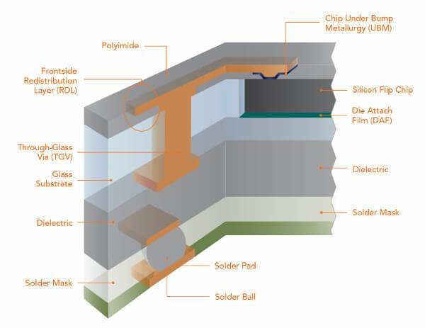
In this example of FOWLP, the silicon flip chip is embedded into the glass substrate, and the RDL fans out over the chip to a through-glass via. Image: Samtec
Heterogeneous integration
The integration of separately manufactured components into a higher-level assembly provides enhanced functionality and improved operating characteristics. It enables semiconductor device manufacturers to combine functional components from different manufacturing process flows into a single composite device.
Heterogeneous integration is similar to system-in-package (SiP); however, instead of integrating multiple bare dies on a single substrate, multiple IPs are integrated in the form of chiplets on a single substrate. The overall idea behind heterogeneous integration is to combine multiple components varying at the system level in the same package.
These are some of the technology building blocks for heterogeneous integration. Image: ASE Group
High bandwidth memory (HBM)
HBM is a standardized stacked memory technology that provides wide channels for data, both within the stack and between the memory and logic. The HBM-based packaging stacks memory dies on top of each other and connects them using TSVs to create more I/Os and bandwidth.
HBM, a JEDEC standard, vertically integrates multiple layers of DRAM components on the package alongside the application processor, GPU, and SoC. HBM is mostly implemented in 2.5D packages for high-end server and networking chips; it has now moved on to HBM2 technology to address capacity and clock rate limitations in the original HBM version.
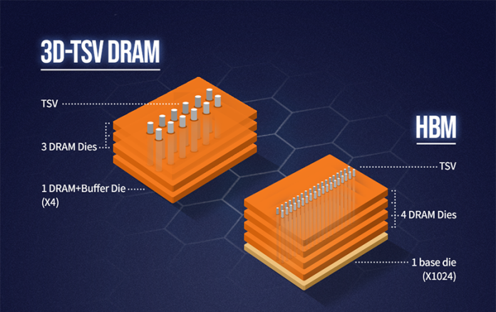
HBM-based packaging stacks memory dies on top of each other and connects them using TSVs to create more I/Os and bandwidth. Image: SK Hynix
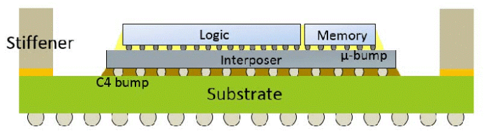
Interposer
It’s a conduit used in multi-chip die or boards to pass through electrical signals in a package. An interposer is an electrical interface routing between one socket or connection to another; it either spreads the signal to a wider pitch or takes the connection to a different socket on the board.
Interposer, which can be made of both silicon and organic materials, acts as a bridge between multiple dies, dies, and board. Silicon interposers, a proven technology, are playing a key role in creating the 2.5D and 3D IC chip packages due to their higher fine pitch I/O density and TSV formation capability.
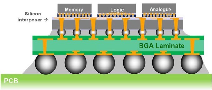
This illustration shows a typical implementation of a system-partitioning interposer. Image: Yole Développement
Redistribution layer (RDL)
Redistribution layers are copper metal connection lines or traces that electrically connect one part of the package with another. RDLs are created with layers of metal or polymer dielectric materials to stack dies on a package and thus relieve the I/O pitch on large chipsets. They have become an integral part of 2.5D and 3D packaging solutions for providing communication between chips attached through the interposer.
These diagrams show an integrated package using a redistribution layer. Image: Fujitsu
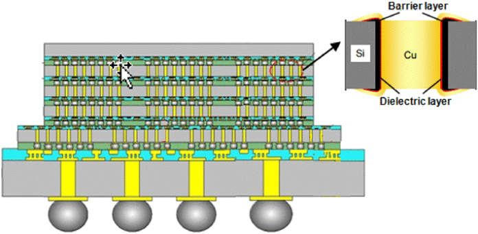
Through silicon via (TSV)
TSV—a key enabling technology in 2.5D and 3D packaging solutions—provides a vertical interconnection that passes through a die’s silicon wafer. It’s manufactured in wafer form and is filled with copper. TSV is an electrical connection through the entire thickness of the chip that creates the shortest possible path from one side of the chip to the other.
The vias or holes are etched from the front side of the wafer to a certain depth, and then, they are isolated and filled by depositing a conductive material, typically copper. After chip fabrication is complete, the wafer is thinned from the back side to expose the vias and metal deposited on the wafer’s back side to complete the TSV interconnection.
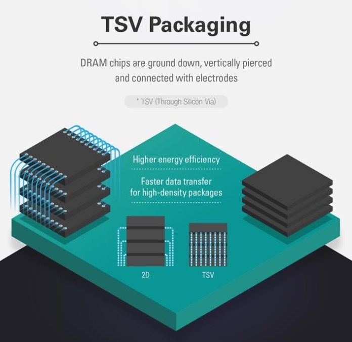
In TSV packaging, DRAM chips are ground down, pierced, and connected with electrodes. Image: Samsung Electronics
This article originally published on sister publication EDN.
Articles in this AspenCore Special Project:
 Heterogeneous integration and the evolution of IC packaging
By Garth Kenyon
The integration of separately manufactured components into a higher-level assembly provides enhanced functionality and improved operating characteristics.
 Tighter integration between process technologies and packaging
By Ravi Mahajan
Advanced packaging technologies improve the performance of heterogeneously integrated IPs on the package and their focus on scaling interconnect densities helps scale bandwidth between die-to-die links.
 Will fan-out wafer-level packaging keep Moore’s Law valid?
By Rich Quinnell
Advanced techniques such as FOWLP allow increased component density, boost performance, and help address chip I/O limitations.
 5 keys to next-generation IC packaging design
By Keith Felton
For many applications, the next-generation IC packaging is the best path to achieve silicon scaling, functional density and heterogeneous integration while reducing the overall package size.
 Wanted: Process Engineers Versed in Packaging
By Junko Yoshida
The new frontier of leading-edge IC design is packaging, according to Arijit Raychowdhury, an expert in digital and mixed-signal design who teaches VLSI courses at Georgia Tech.
 Lost in the advanced IC packaging labyrinth? Know these 10 basic terms
A brief synopsis of the 10 most frequently used terms associated with advanced IC packaging technologies.
For more Special Projects, visit www.eetimes.com/category/special-projects/
Advertisement


