Industrial manufacturers must often attempt to forecast equipment requirements when installing a new system or building a new factory. Projecting communication requirements between new automation systems and existing equipment can be challenging, since requirements or equipment may change over long deployment cycles. Older equipment might use a wide variety of voltage-based communication (±10-V levels, for example), while it’s now common for newer equipment to use current-based communication (for example, 4- to 20-mA loop communication).
To easily adapt to changes in equipment and support both types of communications, industrial manufacturers often prefer to use programmable voltage- and current-output programmable logic controller (PLC) analog output modules to easily transition from one type to another. In this article, we’ll discuss how to design a low-cost discrete programmable analog output circuit that supports both current and voltage outputs on a single connector.

Fig. 1: Simplified voltage- and current-output schematic (Image Texas Instruments) Click for larger image.
Voltage- and current-output selection
In traditional programmable voltage- and current-output designs, a switch such as a multiplexer or metal-oxide-semiconductor field-effect transistor (MOSFET) is used to prevent both output modes from driving the load simultaneously. The design discussed in this article utilized the unique shutdown functionality of the Texas Instruments (TI) OPA2990S, eliminating the need for additional switches in the signal path. Disabling the OPA2990S puts the op-amp output into a high impedance state, preventing the two output modes from driving the load simultaneously. For example, selecting current-output mode disables the voltage-output mode op amps.
Fig. 2 shows the schematic used to control the shutdown pin of the OPA2990S. Because of the threshold voltages of the OPA2990S shutdown pin, this required circuit enables control of that pin with 3-V logic from a microcontroller (MCU) general-purpose input/output (GPIO). The shutdown pin pulls to VDD (3 V), disabling the op amp, with a 0-V input. The shutdown pin pulls to VSS (–15 V), enabling the amplifier, with a 3-V input. To prevent both modes from being on simultaneously, the MCU GPIO control signal for Iout EN and Vout EN must be out of phase from one another.

Fig. 2: Shutdown control circuitry (Image: Texas Instruments) Click for larger image.
Fig. 3 illustrates a second method to control the shutdown pin of the op amp. Using a logic inverter such as TI’s SN74LVC1G04 to invert one MCU GPIO signal ensures that both modes will not be on simultaneously. Although this circuit requires an additional component, it’s a necessity if two logic signals are not available to control the MOSFETs separately.
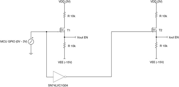
Fig. 3: Alternative shutdown pin control circuitry (Image: Texas Instruments) Click for larger image.
Current-output mode circuit
Fig. 4 is a detailed schematic of the current-output mode circuitry. The circuit converts a 0-V to 2.5-V DAC output voltage to a 4- to 20-mA output current. The circuit is implemented using three stages. The first stage attenuates and level shifts the 0-V to 2.5-V DAC output voltage, the second stage converts the input voltage to a current, and the third stage amplifies the current of the second stage.

Fig. 4: Current-output mode circuit (Image: Texas Instruments) Click for larger image.
Equation 1 expresses the transfer function of the current-output mode circuit:

First stage – level shifting
The first stage contains a voltage divider to attenuate the 0-V to 2.5-V DAC output voltage and uses the internal DAC reference voltage, VREFIO, to level shift the input signal. Generating a 4-mA system output for a 0-V DAC output requires the reference voltage.
Second stage – voltage-to-current conversion
The second stage converts the input voltage to an output current sink. The current sink is accomplished by placing a resistor, Rs1, in series with the N-channel MOSFET to sense the current through the first stage. The voltage drop across the Rs1 resistor, VRs1, is applied to the inverting input of the first op amp. Through negative feedback, the op amp will control the current through Rs1 so that VRs1 is equal to the input voltage, Vin, which is applied to the noninverting input. This sets the current, IRs1 and IRs2, through Rs1 and Rs2. All current through Rs2 flows into ground and is not delivered to the load, reducing the efficiency of the design. It’s important to minimize the current through this stage if high efficiency is a concern [1].
Third stage – current amplification
The third stage amplifies the current of the second stage to produce a 4- to 20-mA output current into the load, R_Load. The second amplifier driving this stage is controlled by the voltage drop across the Rs2 resistor, VRs2, which is applied to the noninverting input. A final sense resistor, Rs3, placed in series with the output P-channel MOSFET produces a voltage drop, VRs3, proportional to the load current that flows through it. The VRs3 voltage is applied to the inverting input, and through negative feedback, the amplifier will set VRs2 and VRs3 to be equal. This sets the current, IRs3 and Iout, through Rs3 and R_Load [1].
With a DAC output voltage of 0 V, pulling the input of the third-stage op amp to Vcc turns off the transistor, T1. Therefore, the one key requirement of the op amp is to have a common-mode input-voltage range that extends to Vcc, otherwise known as a rail-to-rail input amplifier. The OPA2990S meets this requirement.
When the current-output mode is disabled, the op-amp output becomes high impedance. In noisy environments, it may be possible for the transistor to turn on. Therefore, adding a pullup resistor, Rp, to the gate of the P-channel MOSFET transistor can help ensure that the transistor gate pulls high when the current-output mode is disabled.
Fig. 5 graphs the output signal of the current-output mode circuit for a 0-V to 2.5-V input. The current-output mode circuitry is enabled and the voltage-output mode circuitry is disabled. The output current through the load resistor is from 3.97 mA to 20.1 mA.

Fig. 5: Output current vs. DAC output voltage for a current-output mode circuit (Image Texas Instruments) Click for a larger image.
Voltage-output mode circuit
Fig. 6 is a schematic of the voltage-output mode circuitry. The circuit converts a 0-V to 2.5-V DAC output voltage to a –10-V to +10-V output voltage. The circuit is implemented using two blocks. The first block amplifies and offsets the 0-V to 2.5-V DAC output voltage. The second block isolates the feedback resistors, R3, R4 and R5, from the current-output mode circuitry.

Fig. 6: Voltage-output mode circuitry (Image Texas Instruments) Click for larger image.
Equation 2 expresses the transfer function of the voltage-output mode circuit:

Voltage amplification and offset
The voltage amplification and offset block uses a modified summing amplifier configuration to produce a –10-V to +10-V output signal. When the DAC output voltage is 0 V, the inverting terminal is a virtual ground, so no current will flow through R3, causing the circuit to function as an inverting amplifier. With a DAC output voltage equal to VREFIO, the inverting input is equal to VREFIO. No current flows through R4, causing the circuit to function as a noninverting amplifier.
Feedback isolation
The feedback isolation block isolates the feedback resistors, R3, R4 and R5, from the current-output mode circuit. When the current-output mode is on, R3, R4 and R5 will appear as an additional load and steal current from the load resistor, RLoad, which can create significant errors. Placing the amplifier, U2B, in a buffer configuration to produce a high-impedance input eliminates this potential error.
Fig. 7 displays the output signal of the voltage-output mode circuit for a 0-V to 2.5-V input. The voltage-output mode circuitry is enabled and the current-output mode circuitry is disabled. The output voltage at the load resistor is from –10 V to +10 V.

Fig. 7: Output voltage vs. DAC output voltage (Image Texas Instruments) Click for a larger image.
Compensation components
Resistors R7 to R11 and capacitors C1 to C3 are required to stabilize the amplifier due to the gate capacitance of the transistors, T1 and T2, and the possible capacitive load, CLoad, due to cables, connectors, or sensors. Fig. 8 is a detailed schematic with all compensation components included in the design. Although the selection of these components is beyond the scope of this article, for information about sizing these components, see the TI Precision Labs videos on stability.
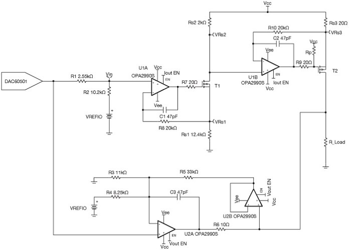
Fig. 8: Detailed schematic with compensation components (Image Texas Instruments) Click for larger image.
Conclusion
It is possible to design a low-cost, discrete programmable DAC output circuit that supports both current and voltage output on a single node. The circuit alternates between current-output mode and voltage-output mode using the shutdown functionality of the OPA2990S, which is controlled with an MCU GPIO pin.
The current-output mode, which can produce a 4- to 20-mA output current at the load, comprises three stages, which include level shifting, voltage-to-current conversion, and current amplification. A pullup resistor in the third stage may be necessary in order to ensure proper operation in noisy environments.
The voltage-output mode, which can produce a –10-V to +10-V signal, comprises a voltage amplification and offset block, as well as a feedback isolation block, which prevents the feedback resistors from stealing current from the load when the current-output mode is selected. This design enables flexibility for numerous industrial applications requiring industry-standard voltage and current communication protocols.
References
- Texas Instruments. n.d. “High-Side V-I Converter, 0-2V to 0-100mA, 1% Full Scale Error.” TI reference design No. TIPD102. Accessed Dec. 4, 2020.
- Texas Instruments. n.d. “Bipolar ±10V Output from a Unipolar DAC for Industrial Voltage Drivers.” TI reference design No. TIPD125. Accessed Dec. 4, 2020.
About the authors
Tim Claycomb is an applications engineer at Texas Instruments. At TI, Tim has worked in the precision amplifier and general-purpose amplifier product lines, where he has supported audio amplifiers, and low- and high-voltage CMOS amplifiers. He holds a bachelor’s degree in electrical engineering from Michigan State University.
Ryan Small is a systems manager at Texas Instruments. Hailing from Edmond, Oklahoma, Ryan earned his BSEE from the University of Tulsa before joining TI through the sales rotation program. He began work full-time as a product marketing engineer in various groups, and he now manages a product definition team for the linear amplifiers group.
Advertisement
Learn more about Texas Instruments


