Sony Semiconductor Solutions Corp. has claimed the first stacked CMOS image sensor technology with a 2-layer transistor pixel. The company’s proprietary technology separates photodiodes and pixel transistors on different substrate layers compared with conventional CMOS image sensors’ photodiodes and pixel transistors that are on the same substrate.
This new architecture approximately doubles the saturation signal level – a single pixel’s maximum electron storage capacity – in comparison with conventional image sensors, widens the dynamic range, and reduces noise. These features substantially improve imaging properties, according to Sony.
The saturation signal level is based on a one square μm equivalent comparison between an existing image sensor and the 2-layer transistor pixel applied to Sony’s back-illuminated CMOS image sensor.
“The new technology’s pixel structure will enable pixels to maintain or improve their existing properties at not only current but also smaller pixel sizes,” said Sony.
“Increasing saturation signal level within form-factor constraints plays an important role in realizing high image quality with wide dynamic range,” added the company.
The new technology is under development first for mobile applications, which will contribute to increasingly higher quality imaging for applications such as smartphones, said Sony.
However, Sony expects the technology to find homes in other applications that require enhanced dynamic range and noise reduction. “As this technology improves dynamic range and low noise, we’re not ruling out any possibility for applications that require this high level of performance,” said Yoko Yasukouchi, Sony Semiconductor Solutions. “We also continue studying further the functional values we’re able to achieve by optimizing the photodiode layer and the pixel transistor layer as well as by increasing the size of the amplifier transistor.”
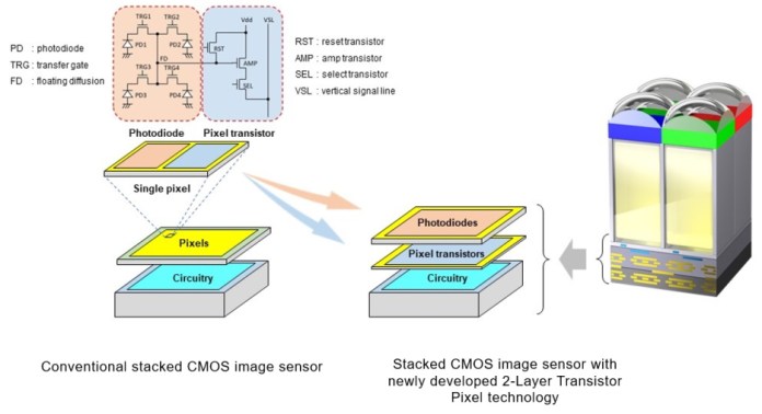
Figure 1: Stacked CMOS image sensor architectures. Click for a larger image. (Source: Sony Semiconductor Solutions Corp.)
Typically, a stacked CMOS image sensor uses a stacked structure consisting of a pixel chip made up of back-illuminated pixels stacked on top of a logic chip where signal processing circuits are formed. Within the pixel chip, photodiodes for converting light to electrical signals, and pixel transistors for controlling the signals are placed next to each other on the same layer.
Sony’s new architecture advances stacked CMOS image sensor technology by enabling the company to package the photodiodes and pixel transistors on separate substrates stacked one atop the other. This allows each of the layers to be optimized, said Sony, delivering a higher saturation level compared to conventional image sensors and a wider dynamic range.
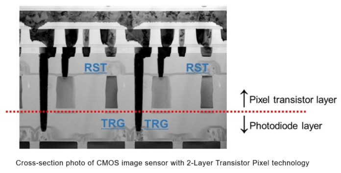
Figure 2: Cross-section of a CMOS image sensor with Sony’s 2-Layer Transistor Pixel technology. Click for a larger image. (Source: Sony Semiconductor Solutions Corp.)
In addition, because pixel transistors other than transfer gates (TRG), including reset transistors (RST), select transistors (SEL) and amp transistors (AMP), occupy a photodiode-free layer, the amp transistors can be increased in size, which substantially reduces noise, which is particularly a problem in nighttime and other dark-location images, said Sony.
The wider dynamic range together with the noise reduction will prevent underexposure and overexposure in settings with a combination of bright and dim illumination (e.g., backlit settings) and enable high-quality, low-noise images even in low-light (e.g., indoor, nighttime) conditions.
Sony announced the new technology at the IEEE International Electron Devices Meeting in December. The company cannot comment on the timing of commercialization.
Advertisement
Learn more about Sony


