A bright future
for chip-scale packaging
Miniature products intensify demand for these small, high-density semiconductor packages
Chip-scale packaging has come into its own as a means for making ever-more-miniature electronic products. Using technologies ranging from wirebonding to wafer-level assembly, the packages can be used to mount a variety of device types.
No longer is chip-scale packaging just a hot topic of conversation at industry trade conferences. A recent marketing study and several product developments indicate that chip-scale packaging is a viable technology whose usage is growing rapidly.
The study, conducted by TechSearch International, an Austin, TX-based technology licensing and consulting firm, predicts that shipments of parts in chip-scale packages are expected to grow sixfold from 1997 to 2000. By the year 2000, chip-scale shipments will reach almost 1.9 billion units.
According to TechSearch, at least 50 chip-scale packages are in various stages of development at some 30 companies worldwide. More than 30 chip-scale packages were expected to be in volume production by the first quarter of 1998.
Most chip-scale packages are being used in Japanese products requiring small size and high interconnection density. Some of the parts being housed in these packages include DSP chips, ASICs, and microcontrollers, as well as various types of memory.
Chip-scale packages currently fall into four categories–flex circuit interposer, rigid substrate, leadframe, and wafer-level assembly (see table ). Within these categories, the technologies used vary from wirebonding to flip-chip molded substrate. The study projects that future chip-scale packages will make more use of rigid or flexible substrates and wafer-level assembly.
| Chip-scale packages worldwide |
| CATEGORY | TYPE | EXAMPLE | COMPANIES |
|
FLEXIBLE CIRCUIT |
TAB flip-chip | GE, IZM, KME, Mitsubishi, NEC, Rohm, Sony, Tessera and licensees | |
| Wire bonding | Amkor/Anam, Fujitsu, Hitachi, Hitachi Cable, LSI Logic, Mitsubishi, Sharp, TI Japan, Toshiba | ||
| RIGID SUBSTRATE |
Flip-chip | Citzen Watch, Fujitsu, Matsushita, Motorola, Oki Electric, Sony | |
| Wirebonding | Not Available | Amkor/Anam, Cypress, Fujitsu, LSI Logic, Motorola, National Semi., NEC, Rohm, Sony, Toshiba | |
| LEADFRAME | Wirebonding | Amkor/Anam, Fujitsu, Hitachi Cable, LG Semicon, Matshita, Samsund, TI Japan, Toshiba | |
| WAFER-LEVEL ASSEMBLY |
Redistribution | ChipScale, WPIC, FCT, NEC, Sandia National Laboratories | |
| Molded substrate | ChipScale and licensees, Fujitsu, ShellCase, Tessera, 3-D Plus |
| Source: TechSearch International |
Two recent developments, from Flip Chip Technologies (Phoenix, AZ) and Amkor Electronics (Chandler, AZ), reflect the diverse approaches being taken. Amkor uses wirebonded die on a tape substrate, while Flip Chip uses a patented wafer-level process (see photos ).
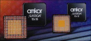
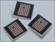
Two recent chip-scale package announcements include Amkor Electronics'
wirebond fleXBGA (left) and Flip Chip Technologies' wafer-level UltraCSP (right).
Amkor's chip-scale package, designated the fleXBGA, is an overmolded, wirebond package similar to a plastic BGA. It is available with 132 to 412 balls on 0.8-, 1.0-, or 1.27-mm pitches. For a package with up to 256 balls, board footprint requirements can be reduced by 40% to 70% compared with a TQFP.
Specifications for the fleXBGA include a minimum inductance of 0.25 nH, a capacitance of 0.13 pF, and a resistance of 5 milliohm. The package is offered in body sizes of 12, 15, 16, and 27 mm, and conforms to the JEDEC MO-195 outline. To expedite production, Amkor has entered into a second-sourcing agreement with Sharp (Osaka, Japan) to produce and develop the package.
Flip Chip Technologies' chip-scale package is the UltraCSP. The patented wafer-level process used in its production results in a price per I/O that is half that of current chip-scale packages. According to the company, the Ultra-CSP is price competitive with older thin-small-outline packages (TSOPs).
The UltraCSP can be used with standard surface-mount assembly and soldering equipment. The package's I/Os can be routed in any fan-in array pattern, including those meeting JEDEC chip-scale packaging standards. In reliability tests, the package has passed 500 cycles of life tests over a –40° to +125°C range. The UltraCSP is available in pitches of 0.50, 0.65, 0.75, and 0.85 mm.
Like Amkor, Flip Chip Technologies is entering a joint manufacturing agreement, this one with XeTel, a surface-mount contract assembly house located in Austin, TX. XeTel will design, prototype, and assemble pc-board assemblies with Flip Chip's UltraCSPs.
For more information on Amkor's fleXBGA, call Christy RePinec at 602-821-2408, ext. 7705, visit http:// www.amkor.com . For more on Flip Chip Technologies' Ultra CSP, call Tracy Schofield at 602-431-6020, ext. 252, visit http://www. flipchip.com . For more on TechSearch International's study, call Tom Goodman at 512-372-8887.
–Spencer Chin
Advertisement


