By YAJUNG TU
Product Applications Engineer
Analog Devices
www.analog.com
Laser diodes are used in fiber-optical telecommunication systems as transmitter lasers for sending signals, pump lasers for erbium doped fiber amplifiers (EDFA), and semiconductor optical amplifiers (SOA). In these applications, the characteristics of the laser, including wavelength, average optical power, efficiency, and extinction ratio have to be kept stable to ensure the overall performance of the telecom system. These characteristics, however, depend on the laser’s temperature: as long as the temperature drifts, the wavelength will change and the conversion efficiency will degrade. The required temperature stability ranges from ±0.001°C to ±0.5°C, differing between applications.
A loop composed of a thermistor, a thermoelectric cooler (TEC), and a TEC controller is needed for temperature control. Because the thermistor’s resistance changes proportionally with the temperature (either negative or positive proportionality, depending on the type of thermistor), it can be used to convert the temperature into voltage when configured as a voltage divider. The TEC controller will compare this fed-back voltage with the reference voltage, which represents the target temperature, and then adjust the amount of heat the TEC has to transfer by controlling the current flowing through it.
The general diagram of the system described above is shown in Fig. 1 . The laser diode, TEC, and thermistor sit inside the laser module. The TEC controller ADN8833 or ADN8834 will read the feedback voltage from the thermistor and provide driving voltage to the TEC. A microcontroller is used to monitor and control the thermal loop. Note that the thermal loop can also be constructed in analog circuitry. The ADN8834 has two built-in, zero-drift chopper amplifiers that can be used as PID compensators.
This article will describe the composition of the thermal control system for laser diodes in telecom systems and introduce the key specification of the main components. The purpose is to walk through the design consideration from a system-level perspective, providing the designer with an overall guideline of how to build a high-performance system with good temperature control accuracy, low loss, and small size.
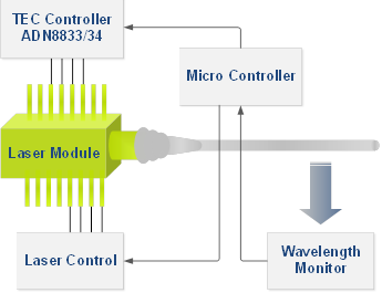
Fig. 1: Temperature control system for laser module.
Thermoelectric cooling
TEC technology
A TEC consists of two surface ceramic plates and an array of alternately placed P-type and N-type semiconductors in between, as shown in Fig. 2 . When current flows through these semiconductors, heat will be absorbed at one end and be released at the other end, and when the current direction is reversed, the heat transfer reverses as well. This process is called the Peltier Effect. The carrier in the N-type semiconductor is an electron; therefore, its carrier and heat flows from anode to cathode. The P-type semiconductor on the opposite has hole carriers and the heat also flows in the opposite direction. Taking a pair of P-N semiconductors and connecting them with metal plates, as in Fig. 3 , the heat will be transferred in one direction as the current flows through.
The heat transfer direction is reversible by changing the polarity of the dc voltage, and the transferred amount is proportional to the voltage amplitude. With its simplicity and robustness, thermoelectric cooling is applied to a wide variety of applications for thermal conditioning in telecommunication systems.
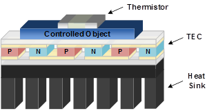
Fig. 2: TEC Module with heat sink.
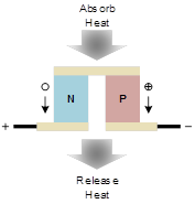
Fig. 3: Peltier Effect: Heat flow of a P-N semiconductor pair.
Selecting a TEC module
There are many factors in the system to be considered when selecting TEC modules, such as ambient temperature, target object temperature, heat load, supply voltage, and physical characteristics of the module. The heat load has to be carefully estimated to ensure the selected TEC module has enough capacity to pump the heat from the system to maintain the target temperature. The TEC module manufacturer usually provides two performance curves in the data sheet; one shows the heat transfer capacity at different temperature deltas (∆T) over supply voltage, and the other shows the cooling/heating current required under different combinations of supply voltage and ∆T. The designer can estimate the module’s power capacity and determine whether it’s sufficient for a specific application.
TEC controller operation and the system design
To compensate the temperature with a TEC, the TEC controller should be able to generate a reversible differential voltage according to the feedback error, while providing proper voltage and current limits. A simplified system block diagram of ADN8834 is in Fig. 4 . The main functional blocks include a temperature-sensing circuit, an error amplifier and compensator, TEC voltage/current sense and limit circuits, and a differential voltage driver.
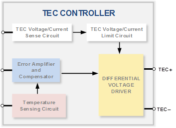
Fig. 4: The block diagram of a monolithic TEC Controller ADN8834.
Differential voltage driver
The TEC controller outputs a differential voltage so that the direction of the current fed through the TEC can pump heat away from the object attached to the TEC, or smoothly change to the opposite polarity to pump heat into the object. The voltage driver can be a linear mode, a switch mode, or a hybrid bridge of these two types of drivers. The linear-mode driver is simpler and smaller but has poor efficiency. The switch-mode driver, on the other hand, has good efficiency — up to more than 90% — but requires additional filtering inductors and capacitors at the output. The ADN8833 and ADN8834 use a hybrid configuration, with one linear-mode driver and one switch-mode driver, reducing the bulky filtering component count by half while retaining high-efficiency performance.
The voltage driver design is critical to the controller since it accounts for most of the power consumption and circuit board space. An optimal driver stage can help minimize the power loss, circuit size, the need for a heat sink, and the cost.
Temperature sensing with NTC thermistors
Fig. 5 shows the impedance of a negative temperature coefficient (NTC) thermistor over temperature. Because of its temperature dependency, it can be used to transfer temperature into voltage when connected as a voltage divider. A typical connection is shown in Fig. 6 ; the VFB varies as RTH changes with temperature. By adding RX in series with the thermistor, the temperature-to-voltage transfer function can be linearized in respect to VREF as shown in Fig. 7 . It is important that it be tightly coupled to the laser inside of the module case, isolated from external temperature disturbances, so it can sense the temperature accurately.
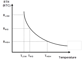
Fig. 5: Impedance curve of NTC over temperature.
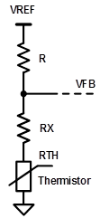
Fig. 6: NTC thermistor connected as voltage divider to read the temperature as voltage.
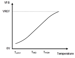
Fig. 7: VFB over temperature.
Error Amplifier and Compensator
The analog thermal feedback loop has two stages composed of two amplifiers as shown in Fig. 8 . The first amplifier takes the thermal feedback voltage (VFB) and converts or regulates the input to a linear voltage output. This voltage represents the object temperature and is fed into the compensation amplifier, where it is compared with a temperature set-point voltage, creating an error voltage that is proportional to the difference. The second amplifier is typically used to construct a PID compensator consisting of a very-low frequency pole and two separate zeroes at higher frequencies, as shown in the figure.
The PID compensator can be determined either mathematically or empirically. To model the thermal loop mathematically requires the precise thermal time constants of the TEC, the laser diode, the connectors, and the heat sink, which are not easy to get. Tuning the compensator empirically is more common. By asserting a step function in the temperature set-point terminal and changing the target temperature, the designer can adjust the compensation network to minimize the settling time of the TEC temperature.
An aggressive compensator reacts to thermal disturbance quickly, but also becomes unstable easily, while a conservative compensator settles slowly, but can tolerate the thermal disturbances with less possible overshoot. It is important to reach a balance between system stability and response time.
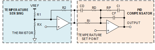
Fig. 8: Diagram of the thermal feedback loop using two chopper amps inside of ADN8834.
Key performances of TEC controller system
Temperature regulation accuracy
Sometimes a steady-state error will still exist, even when the PID compensator is properly designed. There are a few things that might contribute to this error:
- TEC thermal power budget: TEC and the supply voltage are two of the first things selected when designing the system. However, the selection may not be correct because the heat load is not easy to estimate. In some cases, when the maximum electric power has been applied to the TEC and it still can’t meet the target temperature, it might imply that the thermal power budget isn’t enough to handle the heat load. Increasing the supply voltage or selecting a TEC with a higher power rating can resolve the issue.
- Voltage reference consistency: The voltage reference will drift with temperature and time, which usually isn’t a problem if the thermal loop is closed. However, especially in digital control systems, the voltage reference of the TEC controller and the microcontroller might drift differently, thus causing an error that the compensator won’t see. It’s recommended to use the same reference for both circuits, using the voltage with higher driving capability to overwrite the other one.
- Temperature sensing: Sensing the load temperature precisely is critical to minimizing temperature error. Any of the errors coming from the feedback will be introduced to the system and can’t be corrected by the compensator. Use a high-precision thermistor and an auto-zero amplifier to avoid errors. The placement of the thermistor is also important. Make sure it’s attached to the laser so that it can read the actual temperature it’s controlling.
Efficiency
The driver stage consumes the majority of the power in TEC controller. In the ADN8833/34, the power dissipation of the linear driver is straightforward to derive, given its input-to-output voltage drop and load current. The switch-mode driver loss is more complicated, which can be roughly broken down to the conduction losses, the switching loss, and the transition loss. The conduction loss is proportional to the Rds(on) of the FETs and the DC resistance of the filtering inductor. It can be reduced by selecting low-resistance components. The switching loss and the transition loss depend highly on the switching frequency. With higher frequency, the losses are higher, but the passive component size can be reduced. To achieve an optimal design, trade-offs between efficiency and space must be carefully considered.
Noise and Ripple
The switch-mode driver in ADN8833/34 switches at 2 MHz and the fast PWM switching clock edge contains a broad frequency spectrum, creating voltage ripple at the TEC terminals as well as noise in the whole system. The noise and ripple can be reduced by adding proper decoupling and ripple suppression capacitors.
On the supply voltage rail, the ripple is mainly caused by the discontinuous current chopped by the PWM FETs in the buck topology commonly used for the switch-mode supply. Use multiple SMT ceramic capacitors in parallel to reduce ESR and locally decouple the supply voltage. On the switch-mode driver output node, voltage ripple is caused by the current ripple of the filtering inductor. To suppress this ripple, place multiple SMT ceramic capacitors in parallel from the driver’s output to ground. Since the ripple voltage is mostly determined by the product of the capacitor’s equivalent serial resistance (ESR) and the inductor ripple current: ΔVTEC = ESR · ΔIL . Using multiple capacitors in parallel can effectively reduce the equivalent ESR.
Designing TEC controller systems for laser diodes in telecommunication systems is a complex job. Except for the challenge in thermal accuracy, the package sizes are typically very small and the power dissipation tolerance is low. In general, a well-designed TEC controller should possess the following merits:
- Accurate temperature regulation
- High efficiency
- Small board size
- Low noise
- Current and voltage monitoring and protection
Advertisement
Learn more about Analog Devices, Inc.


