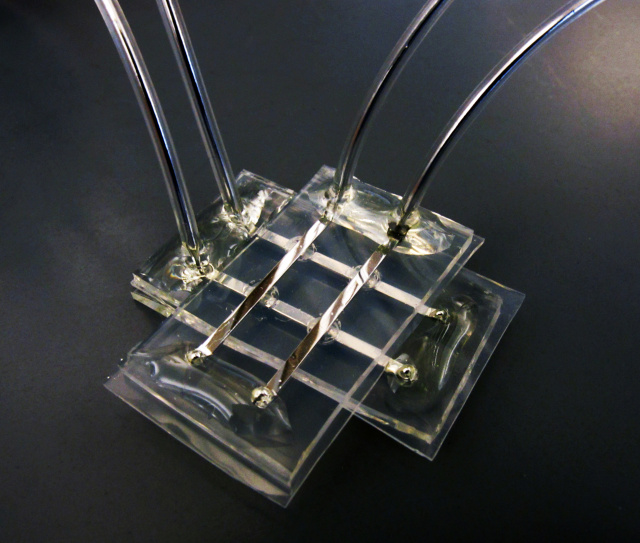
Memory resistors, or memristors for short, are a unique form of circuitry that resemble the neural pathways of the human brain and improve as additional current that passes through them, much like the way neural synapses improve with each subsequent signal passing through them. Although memristors were first theorized in 1971, the closest thing to a functioning prototype chip was only developed in 2008, and even that could do no more than recognize rudimentary simple black-and-white patterns. Fast forward to 2015, and researchers from Stony Brook University — my Alma mater — and the University of California, Santa Barbara, have developed a new method of fabrication that may someday allow the creation of physical neural network on a chip.
Their results are published here.
Software versions of artificial neural networks have existed for quite some time in the form of voice and facial recognition, but computer simulated neural networks are far more resource taxing and highly inefficient: Google once performed an experiment in which 16,000 processors ran for three days before the underlying software was able to learn to recognize cats images it studied because so many transistors are needed to represent a single synapse. On the contrary, physical memristors are far more energy efficient. “Even on a 30 nm process, it would be possible to place 25 million cells in a square centimeter, with 10,000 synapses on each cell. And all that would dissipate about a Watt,” explains Ars’ John Timmer.
But the SBUC team thinks they’ve found a solution: Using a combine of aluminum oxide and titanium dioxide (Al2O3 and TIO2) to form the memristors rather than a single metal oxide. After testing a thorough range of titanium dioxide compositions with corresponding aluminum oxide compounds adjusted for layer thickness, the team found the right layer-thickness combination that then allowed them to create a neural network. By introducing this compound to traditional circuitry linked through a grid of wiring, memristors were able to form at each right angle formed by traditional circuitry arrange in a grid of wiring.
The resulting neural network was then trained to identify the letters V,N, and Z, as well as the possibility of single-pixel errors. Not only did it accomplish this after the first run through the training, but the processing time continuously improved after each attempt. Of course, the system only used a 12-by-12 memristor grid, so capacity was limited, but upsizing the grid will have significant impact.
Robert Legenstein, an associate professor at Graz University of Technology in Austria, writes: “If this design can be scaled up to large network sizes, it will affect the future of computing … Laptops, mobile phones and robots could include ultra-low-power neuromorphic chips that process visual, auditory and other types of sensory information.”
Source: Ars Technica via Nature
Advertisement
Learn more about Electronic Products Magazine


