A new day dawns for solar photovoltaic power
New system architectures, control methods, and device designs promises much more efficient solar power
BY DAN KINZER
Fairchild Semiconductor, Portland, ME
http://www.fairchildsemi.com
People are increasingly aware of the dramatic change in attitude concerning renewable energy in political and economic circles worldwide in recent times. Though some of the strong incentives were curtailed last year in the period of global recession, the market for solar energy installations is expected to grow at a 30% to 40% annual rate for the next several years (see Fig. 1 ).
This growth will be across the range of powers, from the large megawatt central power generating stations to the rooftop residential systems around the world. Efficiency of both the cells and the power electronics are climbing ever higher. At the same time, new topologies and device designs continue to raise the level of performance.
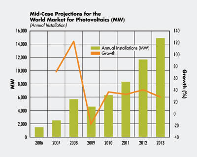
Fig. 1. The market for solar energy installations is expected to grow.
By far the predominant solar cell technology is the single crystal silicon pn junction cell (see Fig. 2 ). This has been the most widely available material, and offers a good tradeoff between cost and efficiency for a broad range of applications. High-power concentrator systems may choose multijunction cells that achieve upward of 25% efficiency, but at much higher cost. Lower-end systems may choose polycrystalline or thin-film systems that offer lower efficiency, but very attractive manufacturing costs.
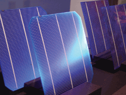
Fig. 2. The predominant solar-cell technology is the single-crystal silicon pn junction.
Typical solar technology
A typical power system consists of two power stages (see Fig. 3 ). The front end is a boost converter that takes the panel output voltage and boosts it to a dc bus voltage that is just high enough to feed power into the line through an inverter.
The input to this system is the solar cell array, which may be a panel, a string of panels, or a parallel and serial combination of panels. Each panel commonly generates a voltage in the range of 50 to 60 V. These are then strung together to arrive at the desired dc voltage prior to the boost.
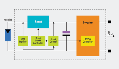
Fig. 3. A typical solar power system has two power stages.
The system also consists of a maximum power point tracking (MPPT) mechanism. Any solar cell or string of solar cells has an output voltage where the power is maximized; lower the voltage and the current doesn’t rise enough to compensate, or raise the voltage and the current drops too quickly. There is typically a computation system that multiplies voltage and current measurements to determine what that maximum power point is and control the output voltage to that value.
In a string of cells, the output current is determined by the lowest output current in the string. If illumination varies or any one cell is partially shaded or obscured, all other cells will be limited and will not operate at their peak output power capability.
There are many ways to compensate for that, depending on the system design. In large central power-generating stations, the cells are usually arranged in large open areas without shade, and often even track the sun to maintain maximum incident isolation at all times.
In smaller systems, however, the arrays can be arranged at different angles to incident sunlight, can be partially shaded, or may just operate at different efficiencies. In such cases, it is desirable to partition the string and operate each partition at the MPP. Then each dc output voltage can be summed. A controller may actually inject a current into weaker partitions to balance and optimize the output current from the entire unit.
New developments
Especially in the field of photovoltaic energy, a new development called a micro-inverter is very promising, since this enables efficiency gains at installation level and helps to exploit all the energy available from each panel. This is gaining popularity in the U.S. for small to medium installations. Here, each solar panel has its own 250 to 500-W inverter attached to it, and this will convert the varying dc input voltage to a constant ac output voltage.
The central inverter can then be designed for a much more narrow input voltage range, driving efficiency upwards, so the gain in output is two-fold. The challenge is to meet the tough environmental conditions at the panel, with high temperatures and strong temperature cycles, so the robustness of the semiconductor products like SupreMOS and Stealth diodes are instrumental to achieving a low failure rate. This usually requires 600-V power devices for single-phase nonisolated operation.
Another approach is to fit each appropriate sized string with an H-bridge inverter, and connect one phase of each inverter to another phase of the next one in the string. In this way, with proper control, the H-bridges can combine to be in essence a multilevel inverter. Since each panel can be isolated from the next electrically, their outputs can be summed and the power device voltage capability can be maintained in a range below 100 V.
Many other topologies are possible and are in use. A three-level inverter places an IGBT and a FET in series between each power rail and the line output. These pairs are then tapped in between and clamped by diodes to the neutral. Such an inverter is gaining popularity for medium to high power, due to its high potential efficiency over 98%.
Another topology popular in larger three-phase installations is the neutral point clamped inverter. This consists of a conventional IGBT inverter bridge with each phase tied to the neutral point through a bidirectional IGBT switch. This topology will typically require the higher power 1200-V IGBT silicon.
Yet another school of thought promotes the current source inverter over the voltage source inverter topologies described above (see Fig. 4 ). The main advantage of this topology is it eliminates the need for the boost and the careful voltage control necessary to feed power back to the line.
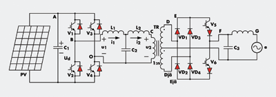
Fig. 4. The current-source inverter eliminates the need for a boost circuit and voltage control.
The IGBT device structure trend is toward thinner silicon- and trench-gated devices (see Fig. 5 ). The original epi-base type with heavy n+ buffer and p+ doped substrate (punch-through type) has largely given way to the thin bulk wafer type with implanted anode (non-punch-through type) and the related field stop thin wafer type with implanted buffer and anode. Backside dopant species and anneal conditions and methods can vary and include diffusion, rapid thermal anneal, and laser anneal. In order to make these structures work, the wafers are so thin they can curl up in the hand (see Fig. 5).
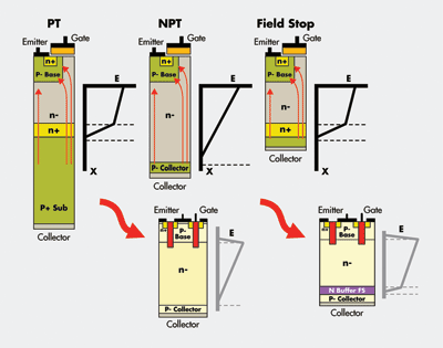
The trend for IGBT device structures is for thinner silicon and trench-gated devices.
For much of the last decade, conventional 600-V MOSFETs have been gradually giving way to a class of MOSFET called super junction. These have traditionally been the type that consist of multiple epitaxial n-type layers with buried p-type layers that merge together to form p-type columns in an n-type background. Devices like the SuperFET are in this class. More recently, a new construction method offers unprecedented performance in efficiency and power density. Deep trench etching and epitaxial filling results in a much denser and lower-resistance FET called SupreMOS devices.
Systems that use local dc/dc conversion can take advantage of the latest concepts in the medium voltage range of 40 to 200-V devices. Devices are now available that are half the size and resistance of conventional trench MOSFETs. This new technology uses a charge balance method to lower the resistance of the epitaxial drain drift region, and a shielded gate to lower the gate-drain capacitance for improved switching and lower losses.
Many designs below 30 kW still use discrete transistors in tried and true TO220 and TO247 packages and the like. However, an excellent lineup of smart power modules in the range of 100 W to 10 kW is available, and can reduce the complexity of system design quite substantially. Most of these incorporate the level shifted gate drive necessary to properly control the power devices in these bridge inverter topologies. The transfer-molded manufacturing method delivers lower heights, reduced materials, and lower costs to the solar power designer.
The continuing revolution in new system architectures, control methods, and device designs promises much more efficient solar power. These improvements, combined with the strong push from governments worldwide to turn to cleaner energy sources, make the future of solar power very bright indeed. ■
Advertisement
Learn more about Fairchild Semiconductor


