Why It’s Important
Prototyping new chips can be an expensive and time consuming process that is finding itself evolving. The race to beat the competition to market has forced manufacturers to speed up development and reduce cost without sacrificing reliability.

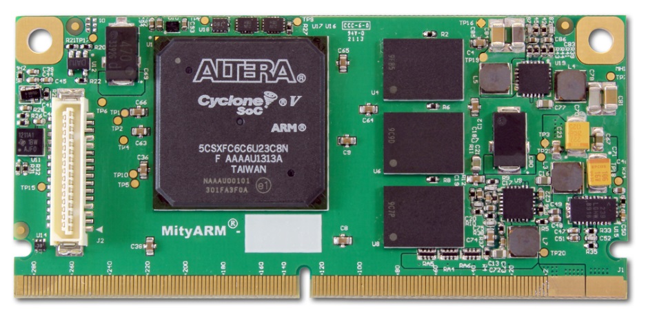
One way to accomplish these lofty goals is through FPGA-based prototyping. FPGA stands for Field-Programmable Gate Array. Prototyping a System on Chip design on a FPGA allows greater reliability in making sure the fundamentals are correct. Most designs are laid out then made to test functionality and reliability. FPGA allows the chip to be made then configured to test functionality.
Nuances of the Technology
There are a few things that make up the architecture of FPGA designed chips and they are: Logic Blocks, Hard Blocks, Clocking, and 3D Architectures. Each one contributes to the unique way these chips are designed and programmed. Logic Blocks require an I/O pad to receive external signals and are considered the most common FPGA architecture. Hard Blocks are a newer architecture that helps reduce the area needed for functions while improving speed.

Clocking is required in FPGA designs due to the synchronous nature of the circuitry. This isn’t an issue though as FPGA designs contain dedicated regional and global networks that are partitioned between FPGA’s.
Some Downsides
FPGA designs were actually slower and more expensive to design up until recently thanks to some new implementations. One of those that improved speed and power consumption was the stacking of architectures. Debugging is also considered a negative when working with FPGA’s due to their nature, especially large ASIC’s and SoC’s. It’s a difficult and time consuming task that eats away at profits. All considered, SoC FPGA prototyping allows manufacturers to mock up, test, and produce the chips in a cost effective way.
Advertisement
Learn more about Electronic Products Magazine


