Accelerating design of >50-W Class D amplifiers
A power switching stage for Class D designs lets you concentrate on amp features and bypass the learning curve
BY JUN HONDA
International Rectifier
El Segundo, CA
http://www.irf.com
Market demands for low-profile designs and high audio output make Class D audio amplifiers very attractive to makers of high-end domestic and automotive audio products. For audio designers, integrated flexible Class D gate drivers eliminate much of the guesswork associated with power switching design.
In Class D operation, the amplifier output transistors switch between the hard-on and hard-off states, allowing the amplifier to operate at >95% efficiency. Compared to typical Class A/B amplifier efficiency of 30%, this improvement reduces heat dissipation and thermal management requirements.
When operated at one-eighth of full rated power, which is considered normal for safety reasons, Class D amplifiers can operate without a heat sink. The overall component count is also lower than for a traditional linear amplifier, allowing designers to achieve high audio outputs within compact case dimensions while reducing build complexity.

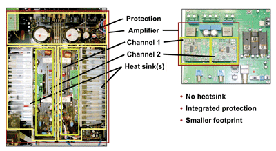
Fig. 1. Board size of 120 W Class A/B amplifier compared to 120 W Class D design.
Figure 1 compares the relative physical sizes of a two-channel linear Class A/B amplifier of 120-W/channel output with a comparable class D reference design. The Class D implementation occupies 61 cm2 PCB area and total volume 109 cm3 , compared to 390 cm2 and 1,794 cm3, respectively, for the Class A/B design.

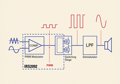
Fig. 2. Typical topology of an open-loop Class D audio amplifier.
Figure 2 shows the basic topology of an open-loop, Class D audio amplifier. The input audio signal is compared with a high-frequency sawtooth wave, producing a square wave that is pulse-width-modulated according to the audio signal. Setting the sawtooth frequency much higher than the maximum audio signal frequency, in the region of 400 kHz, helps to reduce distortion and simplify output filter design.
The PWM-equivalent of the audio signal is then used to drive the amplifier output stage. This may be a full-bridge or half-bridge design, depending on other system requirements including cost, power output, power supply design and signal characteristics. A half-bridge output stage requires positive and negative power supply rails, whereas a full-bridge will operate from a single power supply, produces a higher output for a given switch rating and allows the circuit to be referenced to ground.
Power design for audio engineers
The design of the MOSFET gate-driver circuitry for Class D amplifiers involves power design disciplines that are unfamiliar to many audio engineers. Because a Class D amplifier cannot be turned on gradually, it is difficult to build a finely tuned and well-protected power switching stage. Design flaws can quickly result in catastrophic failure of the circuit that make fault finding at best time-consuming and, at worst, impossible.
On the whole, the power switching stage is difficult to perfect. A plug-in solution may be desirable, to which the designer can add a half-bridge or full-bridge output stage, using MOSFETs optimized for Class D.
This approach allows audio design engineers to focus on other aspects of the amplifier design to differentiate its performance in the marketplace. These aspects include the optimization of the feedback loop to reduce output distortion and the damping factor to achieve the desired acoustic qualities.
Other important features and amplifier properties are closely linked with the power switching stage design, and designers need to have sufficient control over these aspects if they are to deliver outstanding features and maximize value for end users. These include techniques to eliminate EMI caused by the switching stage, the use of a self-oscillating PWM to prevent switching noise from contaminating the audio output, the provision of overcurrent protection, and the implementation of click/pop noise reduction.
Integrated design
New integrated gate driver ICs address these needs and provide flexible building blocks for single- or multi-channel Class D amplifier products in the 50- to 500-W output range. This approach safeguards designers’ freedom to optimize the switching frequency, which also influences the output filter design, and the feedback network.
Feedback design is a crucial differentiating feature for Class D amplifier designs. In some cases, an open-loop configuration may deliver satisfactory performance, but designers can achieve audiophile levels of harmonic distortion and noise (THD + N) performance by judicious use of feedback to improve power supply rejection.
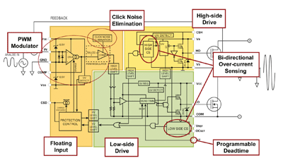
Figure 3 shows a simplified block diagram of the IRS2092 gate-driver IC. The comparator input of the integrated PWM-block can be accessed via an external pin, providing more control over feedback design than is provided by the majority of MOSFET gate drivers.

Fig. 3. Block diagram of the IRS2092 gate-driver IC.
Also, by providing on-chip PWM, the driver IC saves external components and streamlines design, as well as eliminating the EMI challenges associated with external PWM circuitry. Necessary protection features and deadtime control are also integrated, as well as measures to prevent click-noise and switching noise from distorting the output signal. ■
References
Reference design http://ec.irf.com/v6/en/US/adirect/ir?cmd=catProductDetailFrame&productID=IRAUDAMP5
Application note “PCB Layout with IR Class D Audio Gate Drivers” http://www.irf.com/technical-info/appnotes/an-1135.pdf
Datasheet http://www.irf.com/product-info/datasheets/data/irs2092.pdf
Advertisement
Learn more about International Rectifier


