You can obtain precise measurements by using equipment commonly found in any wafer test lab
BY JOHN T. ANDREWS
Fairchild Semiconductor
Portland, OR
http://www.fairchildsemi.com
Resistance measurements are usually straightforward. However, for very low resistance measurements, we need to be careful about the assumptions we make.
The Kelvin technique is very accurate for certain geometries such as wires. A similar method, but different formulas are used for measuring bulk and sheet resistivities of uniform samples. In these cases, the probe spacing and sample thickness must be taken into account.
Simply using a Kelvin connection does not guarantee accuracy. It is difficult to accurately predict what the resistance of a non-uniform geometry will be when the placement and number of connections change.
One of the most important characteristics of a MOSFET is the drain to source on-resistance (RDS(on) ). It is easy to measure RDS(on) after packaging, but there are advantages to measuring it in wafer form.
Wafer-level measurement
For accuracy in any Kelvin resistance measurement, there are several important factors to consider: (1) the geometry of the device under test (DUT), (2) the connections to that device, (3) the material boundaries, and (4) the bulk resistivity of the various materials (including connections).
A typical approach for measuring RDS(on) is to force current between the chuck and the probes contacting the top of the wafer. Another approach uses probes instead of a chuck on the back side of the wafer. This method can be accurate down to 2.5 mΩ.
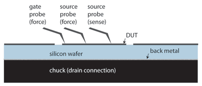
A significant source of error is the contact between the wafer and the chuck (see Fig. 1 ). Because there is roughness on the chuck and on the back of the wafer, electrical contact is made in discrete areas. The contact resistance between the wafer and the chuck is large enough to introduce significant error in the RDS(on) measurement. Simply repositioning the wafer on the chuck will change contact areas and change the RDS(on) measurement results.

Fig. 1. Typical measurement setup, cross-sectional view.
Another source of measurement variation is probe placement. If the current-forcing probe is moved, the current distribution pattern changes. This changes the voltage gradient pattern and results in a different voltage at the voltage-sensing probe.
The adjacent-die method
The required equipment is (1) a probe station with six available probes, (2) a volt meter, and (3) a current source. It is important to insulate the wafer from the conductive chuck. If the wafer contacts the chuck, then it allows current to flow in parallel with the substrate, changing the measurement results. A sheet of paper may be used to insulate the wafer from the chuck.
The connections to the drain are achieved using adjacent, identical devices on opposite sides of the DUT. The internal wafer structure is much more consistent than the connection between a wafer and a chuck. For this reason, the adjacent-die method is much more precise than conventional methods of measuring RDS(on) .
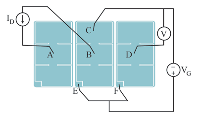
Figure 2 illustrates the measurement setup. The three MOSFETs and six probes are shown graphically, while the electrical connections are shown schematically. The center MOSFET is the device under test.
The polarities shown are for an n-channel MOSFET. The drain current is limited by the current carrying capability of the probes. The MOSFET on the left is used to force current to the drain side of the DUT. The MOSFET to the right of the DUT is used to measure drain voltage.

Fig. 2. RDS(on) measurement setup.
In a MOSFET, when the gate is turned on, and there is no current flowing from drain to source, the drain and source are at the same voltage. This method takes advantage of that principle to measure the drain voltage on probe D.
The gate bias voltage is connected between probes C and E. If it were connected between probes B and E, then the voltage drop between probe B and the source pad would decrease the actual gate voltage applied to the DUT. Since no current flows in the gate during RDS(on) measurement, there is no voltage drop on probe C.
This adjacent-die method does require the MOSFET on the right (under probes D and F) to be functional. If the gate and source are shorted on this die, then the measurement result may not be correct.
The RDS(on) value is calculated by Vdc /IAB , but an even more accurate value of RDS(on) can be obtained.
FEA helps find the RDS(on)
Although the adjacent-die method is precise, it does not yield an exactly accurate measurement of RDS(on) . To find the RDS(on) contribution due to the active area alone, we can compare the measurement results to simulations.
Finite-element analysis (FEA) software can be used to model the measurement setup. Once the relationship between the active area resistance and the RDS(on) measurement is established, we can determine the resistance of the active area, given the measurement result.
The simulation model is a three dimensional representation of the three MOSFETs and a portion of the wafer.
In the finite-element model, the active area resistance is known. The FEA software is used to model the test setup and calculate an RDS(on) measurement result.
The simulation is run twice to obtain results using two different active area resistance values. Since the response is fairly linear, the choice of resistance values is arbitrary. The simulations only need to be performed once for each die size.
Using the relationship between the simulated measurement result and the actual active area contribution, we can derive a formula to find the active area resistance, given the measurement values from the adjacent-die method.
The adjacent-die method
Several factors introduce variation into the measurements. The most significant factors are probe placement, and substrate resistivity.
According to the simulation results, some factors have very little effect on the measurement. The substrate thickness is typically 200 μm. Varying it from 175 to 225 µm only results in a 1% error in RDS(on) (simulated measurement). Also, variations in the back metal sheet resistance will not change the results more than 1%. A surprising result from simulations is that variations in top metal thickness and resistivity also have negligible effects on results.
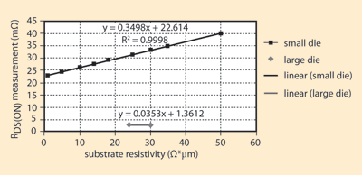
Variations in substrate resistivity result in a linear response in RDS(on) measurement. Figure 3 shows results from substrate resistivities that are well beyond the normal distribution of actual substrates. This was done to show that the response is linear.

Fig. 3. Variation in simulated measurements due to substrate resistivity.
The probe placement on the DUT must be consistent. Variations in probe placement will result in changes in measurement. Probe placement on the device to the left and the right of the DUT (labeled A and D in Fig. 2) also affect measurements, but not to the same degree. The cause of this measurement variation is the fact that the sheet resistance of the top metal is greater than zero.
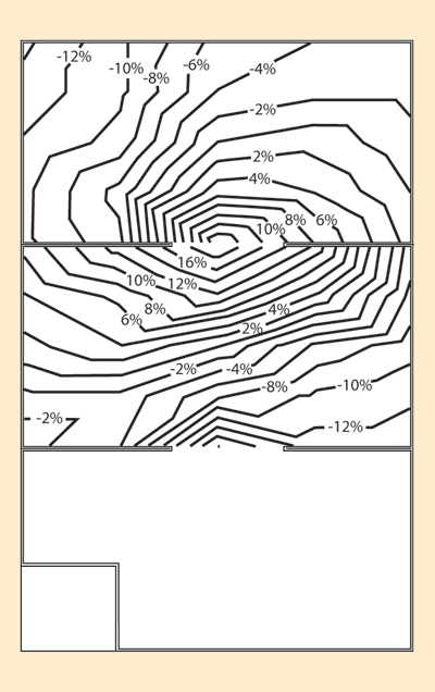
Moving either probe B or C from the center to an edge of the source pad can result in a significant error. Figure 4 shows the error from moving either probe B or C. Each line represents a 2% error in RDS(on) . A 5 x 5-µm grid of probe placements was used to create the plot. Only one probe was moved out of position at a time.

Fig. 4. Error resulting from probe placement.
The adjacent die method is a cost-effective and accurate method to measure the RDS(on) of the active area of a MOSFET in wafer form. It is especially useful in detecting differences between groups of wafers. ■
For more on power MOSFETs, visit http://www2.electronicproducts.com/Semiconductors.aspx.
Advertisement
Learn more about Fairchild Semiconductor


