BY MICHAEL JACKSON, Analog IC Design Engineer, and
SEAN LONG, Director, Applications for the Industrial and Healthcare Business Unit
Maxim Integrated
www.maximintegrated.com
Serial Peripheral Interface (SPI) is an inter-device bus protocol that provides fast, synchronous, and full-duplex communication between a master and one of several slave devices. The master device — such as an MCU or FPGA — drives the clock and selects a slave device, such as an ADC or digital output driver, to address.
Every SPI device consists of a single shift register and control circuitry so that the selected device can simultaneously transmit and receive signals. There are four signals used in SPI communication, as shown in Fig. 1 :
• SCLK: The synchronous clock used by all devices. The master drives this clock and the slaves receive it. Note that SCLK can be gated and doesn’t need to be driven between SPI transactions.
• MOSI: Master Out, Slave In. Also called DO on the master or DI on the slave. This is the main data line driven by the master to all slaves on the SPI bus. Only the selected slave clocks data from MOSI.
• MISO: Master In, Slave Out. Also called DI on the master and DO on the slave. This is the main data line driven by the selected slave to the master. Only the selected slave may drive this signal.
• CS: Chip Select. This signal is unique to each slave. When active (generally low), the selected slave must drive MISO based on SCLK transitions.

Fig. 1: The master and slave SPI connection.
Isolation design challenges
For many industrial control applications, the communication pathway between the digital processor core (MCU) and the I/O module devices must be isolated. Isolation helps to minimize noise and ground loop problems. Moreover, it provides protection for expensive control units like MCUs and FPGAs.
The traditional approach to signal isolation has been to use optocouplers. However, several drawbacks make optocouplers unsuitable for modern, high-speed SPI data transfer applications. Optocouplers are bulky, introduce long propagation delays, and lead to high power consumption. So the smaller CMOS capacitive digital isolation chips have now replaced optocouplers.
However, the use of digital isolators in themselves is not a panacea. For digital isolators to be effectively used in high-speed SPI communication, it is necessary for them to meet several challenging voltage and timing parameters.
Typically, the voltages in the analog and digital domains of the isolator are at different levels. Therefore, for an isolator to be effective, it must be able to operate across a broad voltage range in both analog and digital domains.
Furthermore, since SPI is a de facto standard rather than a formal standard, there is no clearly defined clock frequency. Although many legacy devices may use a clock frequency in the 5–10-MHz range, the newer devices have much faster data transfer requirements, using clock frequencies between 50 and 75 MHz. An effective isolator must be able to operate over this wide SPI frequency range.
By placing a digital isolator between a master and a slave device, additional signal delays are created for the SPI bus. The master uses the rising clock edge to send data and the falling edge to sample the data sent back from the slave.
So the system designer needs to check the timing budget to ensure that the isolator propagation delay does not violate the master’s timing requirements for sampling MISO. Otherwise, the master will lose synchronicity or errors will be introduced into the received and transmitted data, as shown in Fig. 2 .
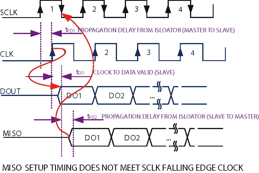 Fig. 2: Timing mismatch due to isolator delays.
A single digital isolator part may consist of several isolation channels — typically between one and four. It is, therefore, critical that the delay is matched between isolator channels. Otherwise, a propagation delay skew may be introduced. So it’s crucial in situations in which, for example, a clock is transmitted via one channel of an isolator and data via another.
Finally, the addition of a digital isolator to the circuit will inevitably cause current consumption to increase. An effective isolator should not contribute excessively to the power budget to avoid heat dissipation in small enclosures.
Addressing voltage and timing woes
Take, for instance, a typical isolated, high-speed SPI communication circuit between an FPGA and an ADC, as shown in Fig. 3 . The ADC is isolated from the FPGA using two digital isolators. SCLK clocks data (MOSI) from the FPGA to the ADC. At the input to the ADC, the isolated SCLK is represented as CLK and the isolated MOSI is represented as DIN.
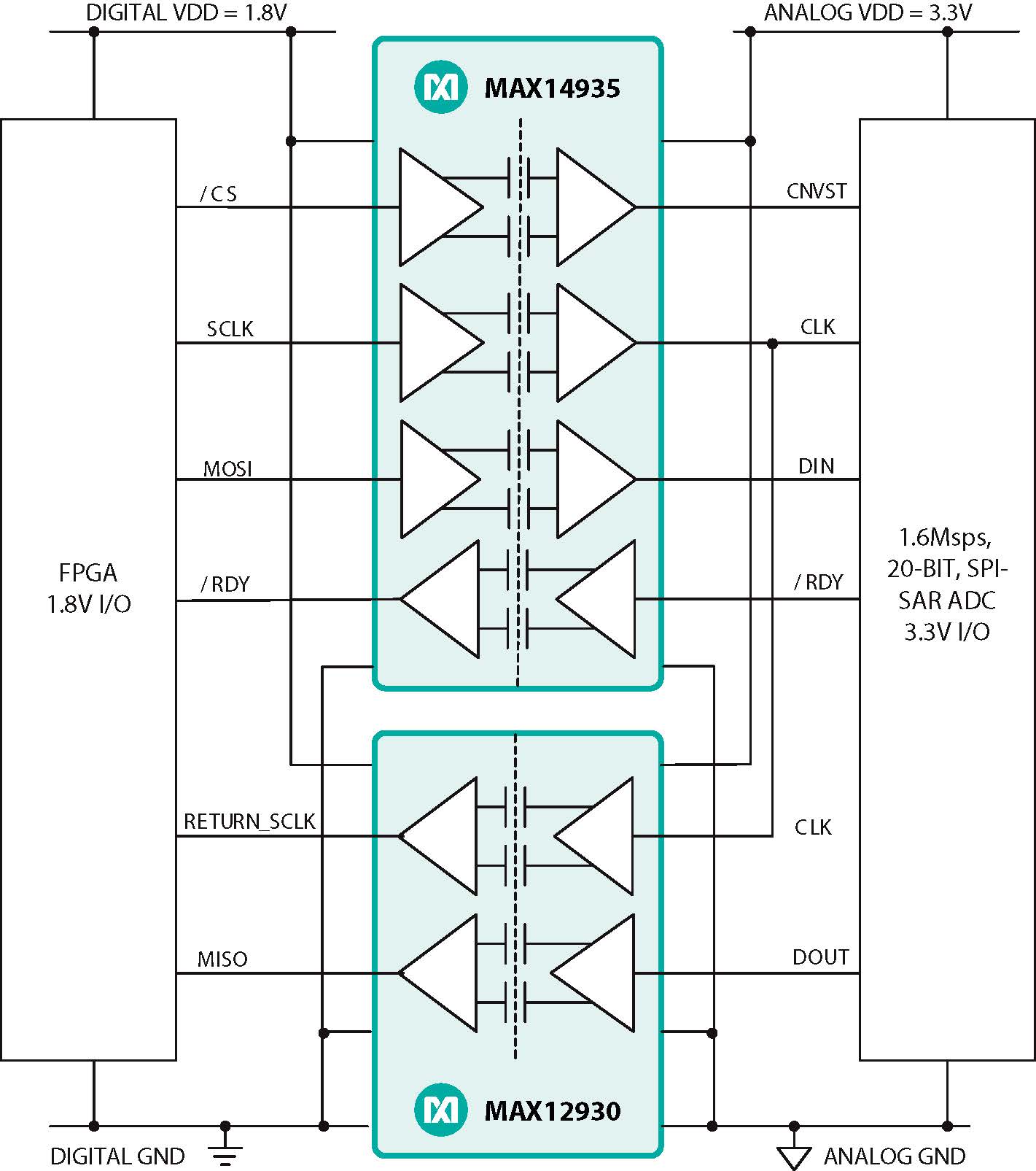
Fig. 3: A typical high-speed SPI isolation circuit.
During low-speed SPI communication, the master clock is also used to clock data (MISO) traveling in the reverse direction. In order to compensate for the fact that the master clock (SCLK) has already been delayed by the isolation in the forward direction, a copy of CLK (the isolated SCLK) is returned when clocking data in the reverse direction from the ADC to the FPGA. It ensures that the timing of CLK and DOUT are still in sync by the time they have been isolated and reach the FPGA as RETURN_SCLK and MISO, respectively.
Hence, for this arrangement to be successful, it is essential to not only have low isolator propagation delay and low channel-to-channel skew but also low part-to-part skew. Therefore, CMOS digital isolators should be specifically designed to meet these requirements and ensure that the circuit arrangement can be implemented successfully to provide isolation in high-speed SPI communications (Fig. 4 ).
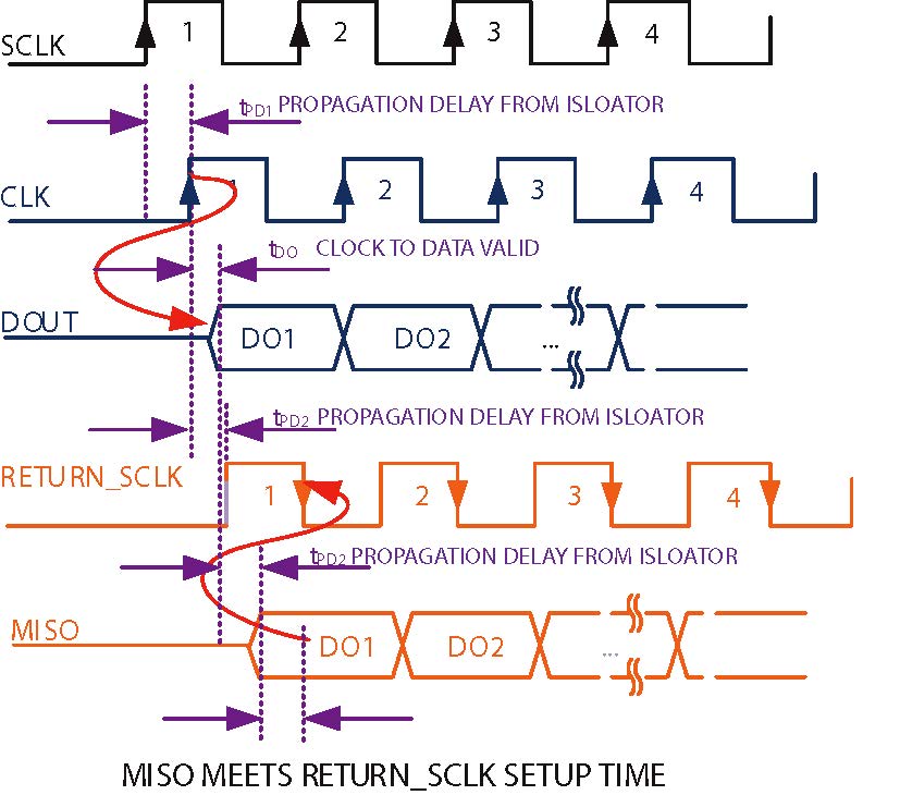
Fig. 4: Timing with clock return to master.
The MAX14934/35/36 and MAX12930/31 families of digital isolators shown in Fig. 3 are based on Maxim’s proprietary capacitive isolation technology. They provide high isolation voltage protection (up to 5 kVrms ) while also supporting data rates of up to 150 Mbps. The parts operate over a wide supply voltage range (1.71 V to 5.5 V) with typical propagation delays of 5 ns (7.5 ns maximum).
A maximum pulse width distortion of 1 ns — combined with a maximum channel-to-channel skew of 0.9 ns and a maximum part-to-part skew of 3 ns — ensure reliable operation in high-speed SPI communication circuits. Moreover, by providing both quad (MAX14934/35/36) and dual (MAX12930/31) options, these digital isolators can also be used in programmable logic controllers (PLCs), telecommunications, and medical instrumentation applications.
Advertisement
Learn more about Maxim Integrated


