By KEDAR BHATAWADEKAR, Product Development and Field Application Engineer, TE Connectivity
Today, all types of port-to-port connections, from personal computing devices to the newest generation of mobile devices, including ultra-thin smartphones and tablets, depend on the USB 3.0 interface’s fast data rate (5 Gb/s) and current and power delivery capability (900 mA), as well as its separate ultra-high-speed “SuperSpeed” data link. Although these enhancements over previous USB interfaces offer faster system performance, they have also intensified the need for more robust ESD (electrostatic discharge) protection in ESD-sensitive USB applications. This article presents a robust ESD protection approach that also helps minimize the impacts to system performance that can result from adding circuit protect devices to high-speed data lines.
ESD protection
A very cost-effective solution for ESD protection in USB 2.0/3.0 applications is to combine an internal ESD protection structure (integrated in the USB transceiver) with a robust, high-current application circuit that is tailored for external ESD protection. This is implemented by the device/circuit designer on the PCB. The internal ESD protection structure is designed to provide device-level protection, according to the HBM JEDEC JESD 22-A115 specification only, which is important for device-handling during development, production and board assembly. More stringent system-level protection, according to the IEC61000-4-2 specification, can be achieved by an external diode tailored to the application.
To achieve a proper system-level ESD protection for USB applications, the ESD protection device must fulfill several different requirements. The ESD performance of a transient voltage suppression (TVS) diode can be ascertained first by the residual clamping voltage and then by the TVS diode response in the case of a dedicated ESD strike, according to IEC61000-4-2.
ESD-protection components are placed on lines that are connected to system I/O connectors, which are usually the ESD entry points. ESD protection components block and divert the ESD current and clamp the ESD voltage to protect the connected ICs. Careful design and placement of ESD protection can not only prevent hard failures, but as a secondary effect they can also help limit the number of soft failures by reducing ESD field coupling as the current is diverted away from sensitive circuits.
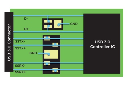
Silicon ESD, or SESD devices, can be placed at the USB power source in USB designs (Fig. 1 ). The product series includes 0402- and 0201-sized devices that have low capacitance of 0.10 pF for bi-directional devices and 0.20 pF for uni-directional devices. They also exhibit low insertion loss that helps provide signal integrity for ultra-high-speed data signals. The single-channel SESD devices provide robust ESD protection with 20kV contact and air discharge rating per the IEC61000-4-2 standard.

Fig. 1: A 4- and 2-channel SESD array in a typical USB 3.0 circuit
Clamping voltage
During an ESD event, a protection device will clamp at its specified clamping voltage and shunt most of the peak pulse current (caused by the event) to ground to protect the device IC from damage. But even with most of the peak pulse current shunted to ground, residual current will still flow into the protected IC. Therefore, the peak pulse during in an ESD event is a combination of the shunted current through the ESD protection device and the residual current flowing into the protected IC. More shunted current through the ESD device will mean less residual current in the protected IC. The power that the protected IC is exposed to during the ESD event depends upon the clamping voltage of the ESD protection device and the residual current. Lower clamping voltage and lower residual current would therefore mean lower joule heating of the protected IC.
Clamping voltage is usually determined by following equation:
VCL = VBR + IResidual (Residual current through protected IC) * RDYN
When comparing different clamping voltages, designers must carefully review the datasheets to understand which test setup was used to determine the value. As designated in IEC 61000-4-2 level 4, an ESD pulse will have a rise time of less than 1ns and a duration of less than 100nS, with a peak current of 30 A. The 8/20µs waveform is designated per IEC 61000-4-4 and is intended for high-power surge events such as inductive kick or lightning surges. An ESD protection diode that shows clamping a voltage of 9 V at (8 /20µs) may actually exhibit a clamping voltage of more than 50 V under ESD testing. Not understanding this, a designer might select an ESD protection device according to the lowest clamping voltage value on the datasheet.
Signal integrity
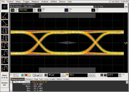
One of the biggest design challenges for ultra-high-speed data transmission systems is ensuring a certain level of signal integrity for a receiver. It is important to achieve a low bit error rate for high signal integrity (a bit error rate of 1E-12 is typical for USB3.0 SuperSpeed). Signal integrity is characterized by the eye diagram, which is produced by repetitively sampling a digital signal on an oscilloscope’s vertical axis while triggering the horizontal sweep with the data rate. The resulting pattern looks like an eye. The larger the eye the better the data signal integrity. In an ideal system without limitations in bandwidth the eye diagram would be completely open.
In an actual system, the signal rise time/fall time is limited by the TX and the RX impedance (90 Ω differential) in combination with all parasitic capacitance at TX side and RX side. These parasitic capacitances are inside the USB3.0 transceiver and/or externally on the PCB.
External parasitics can be caused by unmatched PCB lines, the USB3.0 connector or other shunt capacitors. Therefore it is mandatory to keep these additional shunt capacitors as small as possible. The low-pass frequency response of the USB3.0 cable must be taken in to account as well. To compensate the attenuation of the high frequency content, the signal is tuned by a dedicated equalization on TX and on RX side.
Employing both measures can help speed up the signal at the rising and the falling edge, which results in a more open eye diagram (i.e., improved signal integrity). For a proper signal integrity performance, the capacitance of the diodes must be very low and the diode must provide a high level of ESD protection. The optimum eye diagram performance of a 0.2 pF SESD array device operating at 2.5 GHz is shown in Fig. 2 .

Fig. 2: Eye pattern of an SESD10004Q4UG-0020-090 4-channel array for USB 3.0
Insertion loss
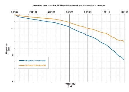
Unlike an eye diagram, the insertion loss plot is created by reference network analyzer test equipment rather than an arbitrary PHY (chipset). A reference test board must be used that has dedicated launches (such as coaxial RF SMA connectors) for input and output. It is extremely difficult to achieve this in an actual system board terminated by a PHY on one end and a USB connector on the other, so these measurements are done by TVS vendors on a reference fixture or evaluation PCB.
For a first-pass evaluation of a TVS device, an insertion loss plot showing Fig. 3 shows insertion loss for 0.2 pf SESD uni-directional and 0.1 pF SESD bi-directional devices. As shown, the insertion loss is negligible at 2.5GHz.

Figure 3. Insertion loss data for SESD unidirectional and bidirectional devices
Summary
USB applications are sensitive to potentially damaging ESD events. A circuit protection solution using silicon ESD devices offers designers robust performance by providing very low clamping voltage and low dynamic resistance. Additionally, the eye diagrams and insertion loss results obtained from device testing, demonstrate the devices’ extremely low impact on logic levels and negligible signal-distortion impact, which is a major consideration in USB applications.
Advertisement
Learn more about TE Connectivity


