By Warren Miller, contributing writer
Applications in the aerospace and defense, test and measurement, communications infrastructure, and high-speed converter markets seem to be forever challenged with several common issues. These complex applications require ever-increasing bandwidth, smaller board space footprints, increased reliability, low noise, and increased clocking range and flexibility.
These capabilities are often competing against each other. For example, higher integration can result in increased noise if internal clocking and regulator circuits aren’t carefully isolated. Increased flexibility results in less precise control of clocking with unacceptable jitter and reference spurious. Operation over a wide temperature range can also impact clocking precision. A next-generation synthesizer from Analog Devices challenges the conventional wisdom that you can’t have it all.
The ADF4371 from Analog Devices, Inc. (ADI) is a state-of-the-art highly integrated synthesizer operating over an RF output frequency range from 62.5 MHz to 32,000 MHz. On-chip resources include a fractional-N and integer-N synthesizer phase-locked loop (PLL), a fully integrated voltage-controlled oscillator (VCO) with four differential clock outputs, and an integrated low-dropout (LDO) regulator. The entire device architecture is highly configurable, using a common three-wire interface to program over 50 control registers. This high degree of programmability makes the ADF4371 appropriate for a very wide range of applications and can be used as the go-to device in wireless infrastructure (MC-GSM, 5G), satellites/VSATs, test equipment and instrumentation, and advanced clock generation applications.
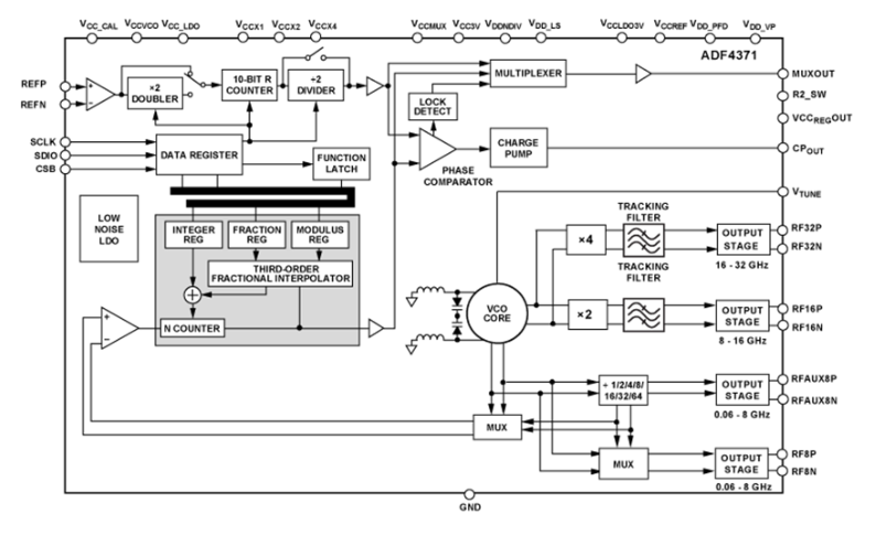
The major blocks of the ADF4371 are shown in the following figure, which shows the VCO at the bottom left of the diagram and the low-noise LDO at the middle left of the diagram. The remainder of the diagram shows the advanced PLL. The heart of the PLL is the programmable third-order fractional interpolator (seen in the middle left of the diagram). It features a high-resolution 39-bit fractional modulus that helps support the wide frequency range.
 ADF4371 ultra-wide-range synthesizer block diagram. Image source: Analog Devices.
The high degree of programmability offered by the ADF4371 doesn’t require performance sacrifices; the advanced clock control metrics listed below will satisfy even the most stringent requirements.
- Typical PFD spurious −100 dBc
- Integrated RMS jitter
- Normalized phase noise floor (FOM) −234 dBc/Hz
- Phase frequency detector (PFD) operation to 250 MHz
- Reference frequency operation to 600 MHz
- Maintains frequency lock over −40°C to 105°C
- Low phase noise, voltage-controlled oscillator (VCO)
- Programmable divide by 1, 2, 4, 8, 16, 32, or 64 output
If your synthesizer application requires a high level of integration, high bandwidth, reliability, a wide temperature operating range, precision operation, and flexibility, the ADF4371 may just be able to let you have it all.
Samples of the ADF4371 (7 x 7 mm, 48-lead LGA) are available now, followed by production availability in September. ADI also offers the ADF4372 (7 x 7 mm, 48-lead LGA) with operation up to 16 GHz, which is sampling now; volume production will follow in October. Both devices are supported by ADI’s ADIsimPLL circuit design and evaluation tool.
Advertisement
Learn more about Electronic Products Magazine


