BY MAJEED AHMAD
Where does advanced packaging stand in 2017? Is it nearing an inflection point? The semiconductor industry is steadily running out of transistor scaling options, so the spotlight is inevitably turning to heterogeneous integration at the package level.
The innovation in packaging technology is also intertwined with the increase in functional density of large system-on-chip (SoC) solutions. So the focus on heterogeneous integration and wafer-level packages (WLP) has led the chip industry to a new set of solutions collectively known as advanced packaging.
It offers greater connectivity and lower power consumption compared to traditional packaging solutions. So they are faster despite the fact that they integrate more die content per package. Not surprisingly, therefore, advanced packaging has become a part of the chip industry's scaling and functionality roadmaps.
According to market research firm Yole, advanced packaging will account for 44% of the packaging industry services while reaching an estimated revenue of $30 billion by 2020. The article chronicles the state of the advanced packaging ecosystem in 2017 and shows how the packaging industry is addressing the key engineering and cost challenges in this realm.
1. Watch out for TSMC's InFO
The fan-out wafer-level packaging (FOWLP) technology is largely being seen as an alternative to 2.5D packaging. Fan-out can manage multiple dies as compared to fan-in wafer-level chip-scale package (WLCSP) technology that handles a single die.
Fan-out, which offers much simpler implementation of heterogeneous integration than 2.5D and 3D packaging, offers smaller form-factors, thinner packages, and higher density I/Os. Moreover, it eliminates the need for process flows such as wafer bumping, fluxing, flip-chip assembly, cleaning, underfill dispensing, and curing.
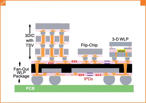 Fig. 1: Fan-out technology is extending to new application categories requiring greater pin counts. Image source: Yole.
Fan-out technology made waves in 2016 when it integrated Apple's 16-nm A10 application processor with mobile DRAM in one package inside the iPhone 7. Apple used TSMC's Integrated Fan-Out (InFO) packaging technology, which the foundry had been developing since 2014.
According to some industry estimates, InFO has improved the A10 chipset performance by as much as 20%. Some media reports suggest that other mobile chipset suppliers — Qualcomm, MediaTek, and HiSilicon — are also considering TSMC's InFO technology for their 10-nm and 7-nm application processors.
Next, OSATs like Amkor and SPIL, as well as IDMs such as Samsung and STMicro, are expected to unveil their fan-out packaging products in 2017. However, when it comes to high-volume adoption of fan-out, the cost is still the elephant in the room.
TSMC's InFO initiative is most likely aimed at creating the economy of scale for fan-out packaging technology. It could bring down the cost and manage processing-centric challenges. For instance, handling signal routes going down to 1 to 2 microns.
2. How to make 2.5D/3D cheaper?
The technology media usually lumps 2.5D and 3D packaging solutions into a single industry jargon, mostly because they stack up multiple dies using interposers like through-silicon via (TSV).
However, 2.5D is an incremental step from traditional 2D IC packaging technology. It's easier to implement in terms of thermal and electrical properties and offers better capacity advantages due to shorter signal routing. In 3D IC packages, two or more dies are mounted on each other in full-fledged vertical mode.
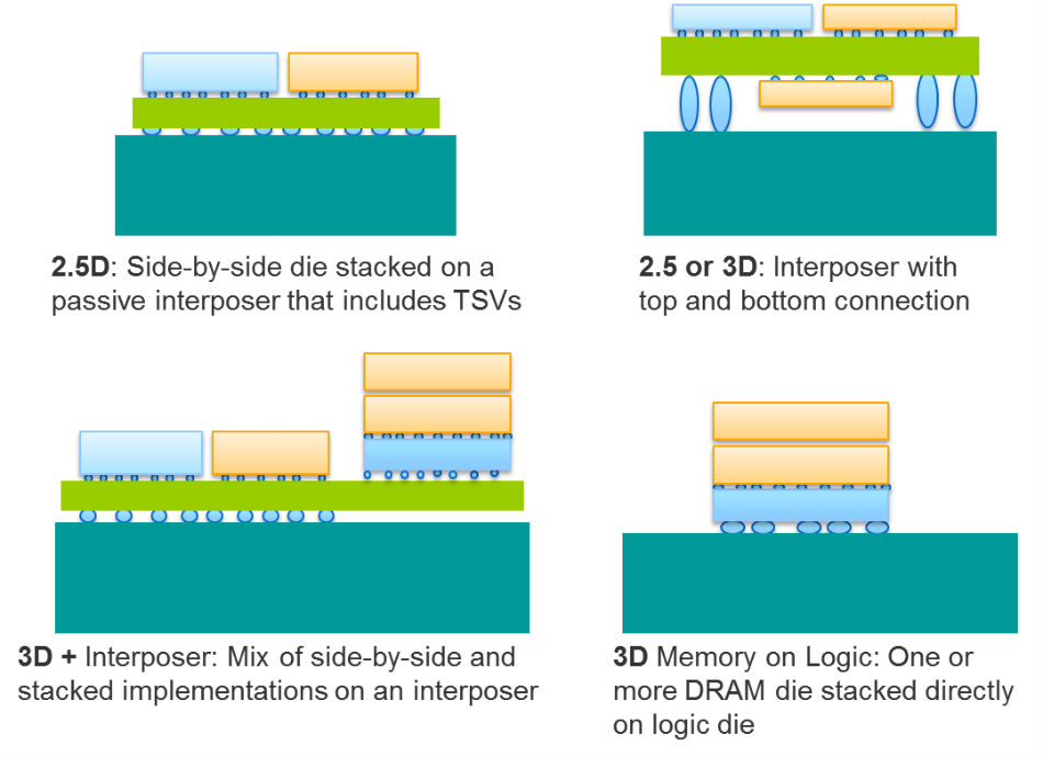
Fig. 2: 2.5D and 3D packaging solutions come in a variety of technical flavors. Image source: Mentor Graphics.
The packaging solutions leverage high-bandwidth memory, high-speed interconnect, and space efficiency to move everything much closer. They stack die using silicon, glass, or organic interposers like TSV to manage communication between the die and the wafer.
However, the proximity of dies in 2.5D and 3D packaging cuts both ways. First, it leads to thermal issues caused by higher levels of integration. Second, warpage, caused by material and temperature differences between die and wafer, can eventually result in chip failures.
Companies like eSilicon are now offering analysis tools for thermal stress and warpage. Expect more tools to manage thermo-mechanical stress issues like materials mismatch during 2017. Still, the biggest challenge remains the high cost of the complex TVS process.
3. Seeking RDL improvements
Redistribution layers (RDLs) are created with layers of metal or polymer dielectric materials to stack dies on a package. The packaging process flow reconfigures chip-level elements as wafers and connects electrode patterns between chips using an interconnect process.
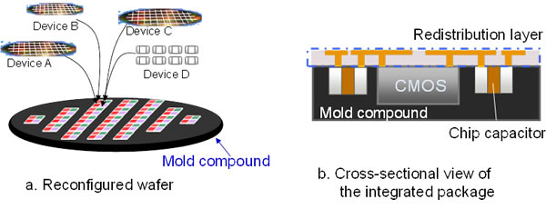
Fig. 3: Fujitsu's RDL packaging combines millimeter-wave signals generated by power amplifiers within an off-chip module.
RDLs relieve I/O pitch on large chipsets that are packed with I/O features and play a critical role in signal distribution among multiple chips. So they have become an integral part of 2.5D/3D packaging solutions for providing communication between chips attached through the interposer.
Likewise, RDLs are created within the die in case of fan-in packages and are done outside the die for fan-out packages. The improvements in RDL technology will bring new levels of efficiency in routing and signal integrity domains. For example, it will be worth watching how mechanical stress is minimized in RDLs.
4. TSV for consumer chips?
TSV is a key enabling technology in 2.5D and 3D packaging solutions. It provides a vertical interconnection that passes through a silicon wafer of a die. TSVs are manufactured in wafer form and are filled with copper.
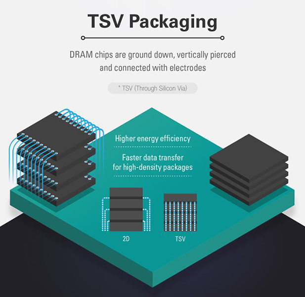
Fig. 4: TSVs pierce hundreds of fine holes through the dies and then vertically connect dies through the holes. That allows for faster data speeds and lower power consumption. Image source: Samsung.
However, cost points are a major obstacle to their use in consumer chip markets like smartphones. So making TSVs cheaper is going to be a major goal in 2017.
Yole forecasts that TSVs will continue to grow in chip packaging markets for high-performance computing, high-end graphics, networking, and datacenters. And TSV could also penetrate into new areas, such as ambient light filters, LED drivers, and RF filters.
5. The next HBM interface
The high-bandwidth memory (HBM) technology has already been implemented in 2.5D packages for high-end server and networking chips from vendors like AMD and Nvidia. Micron has also implemented a similar technology — hybrid memory cube, or HMC — for Intel’s Knights Landing processors.
The fact that Hynix and Samsung have adapted the HBM2 standard spearheaded by JEDEC is considered a huge boost for the 2.5D packaging industry. The HBM2 standard addresses capacity and clock rate limitations in the original HBM version. Take Hynix, which used HBM1 stacks for its 29-nm DRAM dies; the Korean chipmaker later moved to implement HBM2 memory for its 21-nm process.
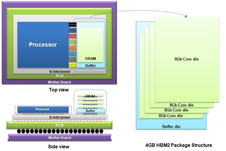 Fig. 5: Samsung’s HBM2 DRAM package features 256 Gbps of bandwidth, thus doubling the capacity of HBM1 DRAM package.
Similarly, Samsung has started producing 4-GB DRAM packages using the HBM2 interface (see Fig. 5 ). And now both Hynix and Samsung are working on the follow-up technology to bring down the higher costs associated with HBM1 and HBM2 packaging. The HBM3 technology also promises to improve the density, bandwidth, and power efficiency of IC packages.
Advertisement
Learn more about Electronic Products Magazine


