Samsung Electro-Mechanics
Seoul, Korea
http://www.sem.samsung.com
The semiconductor is a highly integrated device that cannot be connected directly to the main board in the way that condensers or resistors can. Therefore, a packaging substrate (or intermediary layer) is needed to transmit the IC signals to the main board. In other words, the semiconductor packaging substrate is a support material that acts as a bridge between the semiconductor and the motherboard.
Mobile phones, PDAs, and other mobile products continue to take on new roles such as digital camera, video camera, and TV receiver. These functions require an increased number and greater variety of semiconductors in order to operate, while consumers want their finished products in ever-smaller form factors.
Manufacturers have addressed the problem of diminishing space by applying multichip packages (MCPs), which stack the semiconductors in layers to enable diverse functions. Here too, the industry is demanding thinner IC substrates so that they can stack more chips inside an increasingly restricted space.
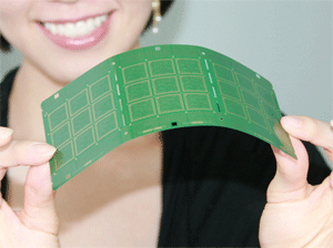
Thus, as mobile phone sales have soared, demand for the chip-scale package (CSP) has increased faster than any other IC package type over the past decade or so. The CSP is already the product of choice for most baseband and memory devices, and an increasing percentage of transceivers and RF modules are packaged in IC substrates. The global market for mobile phones is forecasted to exceed one billion units sold. Each mobile phone uses 5 to 7 substrates, meaning that a market now exists for some 5 billion CSP substrates a year. In addition to the purely numerical growth, the substrates and the chips are being stacked, so 3-D packaging technology is enabling semiconductors to take on multiple functions in smaller form factors. This trend is driving new technologies related to substrates.
Thin substrates
The total thickness of the package poses the greatest limitations on semiconductor packages used in mobile phones. Solder balls are usually included in the connections between the package substrate and the main board, and the total thickness must not exceed 1.4 mm or in some cases 1.2 mm.
The regular CSP contains a single chip, and 100-μm copper-clad lamination will suffice. However, both the highly integrated packages for multiple chips stacked within a single package and double-layer CSP substrates require 60-μm copper-clad lamination; their total thickness is about 130 μm.
This kind of ultrathin package is mainly used with memory chips for mobile phones, and each package normally holds three or four chips. As a result, the mobile phone may retain a small form factor while providing multimedia features such as a video camera and MP3 player.
Samsung Electro-Mechanics recently completed development of a 0.08-mm (80-μm) semiconductor substrate, which is thinner than paper and can be used to stack as many as eight high-performance ICs such as flash memory or static random access memory.
The company has applied a new-concept method called “transferred pattern” to produce these new substrates, which only need a 20-μm space for internal circuitry. This is 20% thinner than the 25 μm required for other substrates. Moreover, Samsung’s new substrate is at least 50% more rigid than the others on the market.
Four-layer CSP substrates for application processors and basebands are showing a similar trend in the marketplace. There are four-layer CSP substrates currently in mass production with 220-μm total thickness.
Fine pitch
The rapid increase in the use of ultrathin substrates has been accompanied by a marked development in patterning techniques. Most makers have achieved the technology to create patterns with line/space widths of 30 μm / 30 μm, but market demand has recently arisen for 25-μm / 25-μm and 20-μm / 20-μm line/space patterns.
Most substrate manufacturers are changing Cu Patterning technology from conventional “subtractive” to “semi-additive” technology, which forms patterns through plating. In a few years, the technology will be available for 15-μm / 15-μm line/space patterns.
Changes are also occurring in the photolithography for creating circuits. The currently common method has been to coat the substrate surface with a light-sensitive polymer (photoresist), place a photomask on top and irradiate with ultraviolet light. This method is highly productive, but it requires the creation of separate photomasks for each model, and each mask must come in various sizes to accommodate the contraction or expansion of the substrate itself.
Recently, innovative technologies have been developed to perform the exposure process with laser direct imaging (LDI) while dispensing with the photomask. Many refinements still need to be made before the technology can be widely applied. For example, a special photoresist for LDI is still required. However, technology will be available that will revolutionize the exposure process within a few years.
Surface finish
Meanwhile the commercially available CSP substrates mainly use gold wire to connect the semiconductor chip to the substrate. Electrolytic nickel/gold provides the most stable finish for this type of wire bonding. A plating line is essential for applying the electrolytic method, and this poses no problem when a single chip is being packaged. However, as the circuitry becomes denser, the plating line grows more complex, restricting the production process.
Therefore, some are suggesting the use of electroless nickel/palladium/gold; the elctroless plating method essentially renders the plating line unnecessary. Wire bonding remains feasible even when the palladium and gold is very thin, and the technique can also be widely used with flip-chip connections.
Flip-chip chip-scale package (FC-CSP)
Cutting-edge 65- and 45-nm semiconductor-processing technologies are now being applied commercially, and CSP connections are changing accordingly. Wire bonding has reached a limit with the faster processing rates, increased number of connections, and smaller chips sizes. Manufacturers are now starting to apply flip-chip connections with chip-scale packages.
The conventional CSP has a gold wire connecting the chip with the substrate. However, the FC-CSP uses solder bumps to make the connections, after which the gap between the chip and the printed circuit board is packed with underfill.
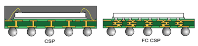
The structure of CSP and FC-CSP
Structure of FC-CSP
The use of solder bumps shortens the length of the connection, providing better electrical properties than can be obtained with the conventional CSP. The resulting integration gains have driven demand for flip-chip chip-scale packages for memory devices as well as processors.
FC CSP packages come in two types—area array connection and peripheral array connection—depending on the position of the connection pads. The area array is used for most baseband devices and application processors, while the peripheral array is preferred for memory chips and certain baseband devices.
The global FC CSP market is estimated to be worth $78 million this year and to achieve an average annual growth of 69% to reach some $370 million by 2010. The FC-CSP requires a more exacting design rule than the wire-bonded CSP does, but it is now being used with high-performance memory, graphics DRAMs and other fast, high-capacity devices.
Future of CSP substrates
The development of semiconductor chips and the increasing complexity of functions have given rise to “embedded die technology” that maximizes the substrate function. This is also the means for further size reductions.
Until now, the technology has been restrictively used to certain chips with few connections. However, companies and research institutions are now working on diverse approaches that promise to revolutionize substrate production processes, bringing them a step closer to commercial viability. ■
Samsung Electro-Mechanics was established in 1973 as a manufacturer of key electronic components, and the company has grown into one of the industry leaders, thanks to cutting-edge technology and top product quality. They directly sells over 80 percent of its own products, operates manufacturing facilities, R&D distribution and sales centers, and offices in the U.S., Europe, Japan, China, and Southeast Asia.
Visit http://cspsubstrate.electronicproducts.com to see full coverage of Chip-scale packagesSponsored by Samsung Electro-Mechanics • www.samsung.com
Advertisement
Learn more about Samsung Electro-Mechanics


