The LTM9011 is a high speed, octal ADC with a serial LVDS interface. Each channel output can be configured in 2-bit (2-lane) mode or 1-bit (1-lane) mode. This document only demonstrates 2-lane mode and 16-bit format (14 bits of data with two dummy bits per frame) supporting the maximum sampling rate up to 125Msps per channel.
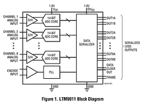
The LTM9011 integrates two quad channel 14-bit ADCs similar to the LTC2175, as shown in the block diagram in Figure 1. The sample clock, ENC±, launches the A/D conversion and the output sample data are carried on two serial data streams. Each 14-bit sample is formatted as 16 bits while the LSBs always contain zeroes. Data bits are synchronized with the bit clock, DCO±, and the sample boundaries are indicated by the frame signal FR±. For more about LTM9011, see the data sheet at http://www.linear.com/product/LTM9011
Download full block diagram below
Advertisement

Learn more about Linear Technology


