As high-brightness LEDs replace traditional light sources, careful approaches are needed for effective thermal management
BY NORMAN QUESNEL
Advanced Thermal Solutions
Norwood, MA
http://www.qats.com
Though cool to the touch, high-brightness LEDs (HBLEDs), with their higher power needs, require direct cooling methods to keep within normal operating temperatures. Without them, the light output of a HBLED will be much shorter than normal.
Inside-out management
HBLED thermal management systems now in use are closer to those used for cooling hot computer chips than incandescent light bulbs. Unlike a light bulb, where most heat will radiate into the air, LED heat management should be considered from the inside out, starting with its semiconductor die junction.
The junction must be kept at or below the maximum rated temperature. Here, thermal control is achieved mainly by conduction. It starts at the junction and ends with natural convection and/or radiation of heat to the ambient.
Unfortunately, the heat transfer from source to ambient is not free flowing. Thermal resistances at different points pose major obstacles. As with other ICs, the highest thermal resistance in the heat transfer path is the junction-to-case thermal resistance (Rj-c ) of the package.
Spreading resistance is also an impediment to thermal transfer. As the power dissipating from HBLEDs increases, and clusters of multiple diodes produce considerable aggregate heat, different kinds of circuit boards are needed. Thermally enhanced spreader materials, such as multilayer FR4 PCBs, ceramic and metal-core boards, cold plates, and vapor chambers are viable systems to reduce spreading resistance.
When high power LED packages are mounted on metal-core (MC) or ceramic PCBs, a specially designed luminaire is need to facilitate heat dissipation. Integral heat sinks (see Fig. 1) improve heat dissipation, and fans can be added if needed.
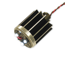
Fig. 1. LEDs are mounted on a fixture with an integral, finned heat sink.
Alternatively, flexible thermal circuits provide heat-spreading properties for mounted HBLEDs. Flex circuits can be installed on curved surfaces, such as along hand rails or walkways, where FR4, MCPCBs, and other rigid materials can’t be used.
An analytical approach
Developing a thermal-management design for high power LEDs is more effective if three steps are taken:
1. Integral analysis
2. Computational analysis
3. Experimental verification
The value of this approach can best be illustrated using an example.
Consider a spotlight used for down-lighting, with white HBLEDs mounted on an MCPCB consisting of a thermally conductive, laminated board with an aluminum base (see Fig. 2). The PCB is mounted on a radial heat sink using a thermally conductive, double-sided adhesive tape.
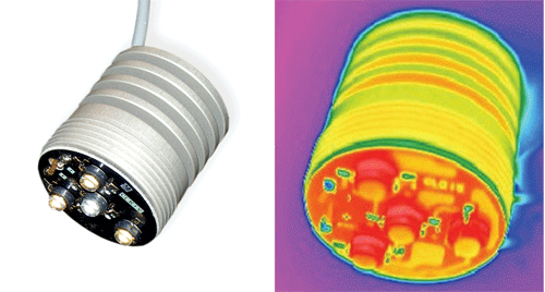
Fig. 2. For the LED-based spotlight at left, an IR image (right) shows thermal properties.
This spotlight application features four 1-W LEDs, each with a junction-to-case thermal resistance of 15 K/W. On the rear of each LED, an aluminum heat slug is used to conduct heat from the junction to the external world. The slug is connected to the board using a thermally conductive compound, in this case thermal glue whose thermal resistance is specified as 4.3 K/W.
For successful cooling, the thermal resistance of the PCB must be considered. Large copper lands on the PCB, directly under the LED slug, improve thermal spreading. The copper’s thickness and area, the thickness and thermal conductivity of the PCB material, and the use of an MCPCB are key to decreasing thermal resistance.
Integral analysis
For a first-order solution, integral analysis identifies the problem areas (components and system layout) and the magnitude of the thermal issue (device junction temperature and required level of cooling). Some analyses can be performed quickly to get the scope of the problemthe so-called “what if” scenario.
The action of the four LEDs mounted on the PCB is best described using an electrical analog (see Fig. 3). Although this is a two-dimensional representation, in most cases it will be sufficient for first-order analysis of the thermal problem.
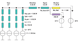
Fig. 3. Heating of an LED lamp can be diagramed using an electrical analog.
The MCPCB is mounted onto the base of a round heat sink using a double-sided, thermally conductive tape. This interface adds a theoretical thermal resistance of 0.3 K/W to the network. The spreading resistance within the base of the heat sink is expected to be zero, since the respective areas are the same. Heat is removed from the sink’s base and fins by natural convection and radiation.
With the total thermal network in place, the junction temperature can be calculated for a specified ambient. When the LEDs are operating on 1.1 W, the junctions are within spec. In this setup, radiation heat transfer contributes 23% and must be included in the analysis. For natural convection cooling, the performance of the heat sink will differ based on the power supplied to the LED.
Computational analysis
Computational analyses were used to develop second-order solutions to verify results from the integral analysis. To develop a model that accurately represents the problem, the problem must be well understood. Computational fluid dynamics (CFD) simulation was used to characterize the spreading resistance, flow around the LED lamp, and heat sink performance (see Fig. 4).
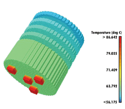
Fig. 4. A CFD simulation of the LED lamp results in the calculated thermal characteristics shown.
The LEDs were represented by compact two-resistor models. The effect of the glue layer interface was added to Rj-b , the thermal resistance between the chip and the heat-carrying layers of the PCB. A detailed model was used for the board to accurately represent the effect of spreading resistance. The heat sink was modeled in greater detail.
Experimental verification
For this application, the junction temperature was measured using the forward-voltage characteristic. All four LEDs were calibrated with a 10-mA current source and, during the operational test, the current measurement source was on all the time. After stabilization, the operational current was switched off.
The resulting drop in forward voltage was measured with a digital storage oscilloscope. The thermal mass of the junction is small, which resulted in a fast cool-down time. This temperature change occurred in less then 1 ms, so the forward voltage had to be measured in microseconds after the event.
Comparing results
The accompanying table shows the results of all three analysis methods. The measurements offer a good comparison of the analytical/computational methods, and the error factor is within 16%. (Detailed measurement results are available on line.)
The interface resistances and thermal spreading showed higher values in the experiment. Interface resistances are theoretically difficult to predict. Only an actual experiment can give the final answer and take account of manufacturing deviations.
Results for different methods
| Parameter | Temperatures Corrected [°C] | ||
| Analytical | Numerical | Experimental | |
| Ambient | 25 | 25 | 25 |
| Heat Sink Base | 63 | 63 | 65 |
| Metal Core | 65 | 64 | not meas |
| PCB below LED | 66 | 65 | 70 |
| Junction | 87 | 87 | 96 |
.
Considering the LED’s junction temperature limit of less than 120°C, and the calculated/measured junction temperatures shown in the table, the results show ample design margin. Therefore, the selected cooling solution (heat sink) is suitable for this application and there is no need to consider a higher-capacity system. ■
Advertisement
Learn more about Advanced Thermal Solutions


