Some secrets to making a highly efficient charger adapter that meets international specs
BY SILVESTRO FIMIANI
Power Integrations, San Jose, CA
http://www.powerint.com
The new generation of cell phones, led by the iPhone, is more feature-rich than ever. Today’s consumers demand large screens, web browsing, GPS, and media players for their must-have full-feature devices, and all of these essential functions require power. The typical handset consumer waits to recharge their cell phone battery until shortly before it has drained, so a fast recharging capability is highly desirable. In addition, cell phone chargers are typically left plugged in when not in use; so, in addition to providing a high charging current at high efficiency, the charger must also consume as little power as possible when left plugged in (under no-load conditions). To design a power supply that can meet these criteria and be economic to manufacture and comply with all EMI requirements, many factors must be considered.
The total amount of electricity consumed in the domestic sector by chargers and external power supplies is significant and has attracted the attention of regulatory authorities around the world. Many countries base their national standards on the Energy Star specifications originating in the United States. The Energy Star EPS v2.0 specification sets a sliding scale for the required efficiency, based on power output. For a 5-W charger, the efficiency must be better than 68%. Meeting this limit is not trivial and will result in a large percentage of chargers offered in the market up to now either being re-designed or withdrawn from sale.
Cell phone manufacturers are also insisting on tighter requirements, seeing energy reduction as a means of demonstrating good corporate citizenship and attracting eco-minded consumers. In late 2008, the five major cell phone manufacturers (Nokia, Samsung, Sony Ericsson, Motorola and LG Electronics) instituted the cell phone charger Star Rating System (http://www.nokia.com/chargerenergy). To achieve the coveted five-star rating, chargers cannot exceed 30- mW power consumption in no-load mode – just one-tenth of the limit currently permitted under Energy Star EPS Specification Version 2.01 (http://www.energystar.gov/).
Meeting the specs
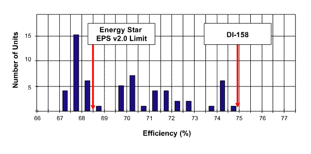
A 5-V, 5-W flyback charger/adapter circuit developed by the Power Integrations(2) achieves an average efficiency of 74% over the load range, a 6% improvement over the Energy Star EPS v2.0 requirement. Figure 1 illustrates the results of testing by Energy Star of 59 different external power supplies. The performance of this circuit was achieved without adding complication to the design and is reproducible in a production environment.

Fig. 1. Efficiency distribution tested on 59 units of EPS (5 V, 1,000 mA) by Energy Star
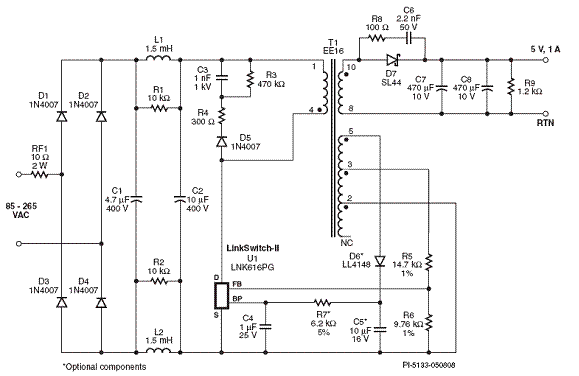
The schematic in Fig. 2 depicts the design for a 5-W universal input, constant-voltage/constant-current (CV/CC) charger/adapter. This design is useful for cell phone battery chargers, USB chargers, or any applications requiring a CV/CC characteristic. The circuit provides a constant 5-V output to an accuracy of ±5% for loads up to 1 A. If a greater load is demanded, the supply moves into constant current mode and the output voltage is reduced to maintain the output current at 1 A ±10%.

Fig. 2. 5-W CV/CC universal input charger power supply
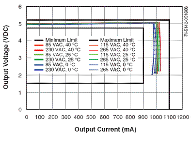
The power supply is a flyback configuration based on PI’s LinkSwitch-II (3) product LNK616PG (U1). This is not a conventional PWM controller, but uses on/off control to maintain regulation in the CV region. The output power level is controlled by skipping switching cycles and regulation is maintained by adjusting both the ratio of enabled-to-disabled switching cycles and the primary current limit. This control scheme provides many unique advantages that are exploited in the charger design. As the load current increases, the current limit is increased and fewer cycles are skipped up to the maximum power point at which no switching cycles are skipped. A further increase in demand for power will then cause the output voltage to drop. The controller senses the voltage drop and transitions to constant current mode. In this mode, as the current demand increases, the switching frequency is reduced to achieve a linear CC output. Figure 3 illustrates the current and voltage performance achieved by the circuit.

Fig. 3. Typical CV/CC characteristic over line and temperature
Elements for efficiency and low cost
Several major elements of the design contribute to high efficiency and low cost. A key element is the transformer T1, the design of which is largely determined by the performance of the switching element in U1. The LinkSwitch-II device has an integrated 700-V power MOSFET as the main switching element. This can operate at up to 85 kHz, almost double the 45 kHz maximum for competing BJT designs. The higher frequency permits a reduction both in the size and number of layers in the transformer; therefore capacitive losses in the transformer are lower. In order to minimize audible noise that may be generated by the transformer, it is important to control the maximum flux density. At the beginning of each switching cycle, the MOSFET in U1 is turned on and the current through the primary winding of T1 ramps up to a maximum value determined by the LinkSwitch-II control circuitry. At this point, the MOSFET is turned off and the energy stored in T1 is transferred to the secondary winding as the magnetic field collapses. At light loads, the primary current limit is reduced to decrease the transformer flux density. The control of the current limit, combined with adjusting the ratio of enabled-to-disabled switching cycles, optimizes converter efficiency over the entire load range by scaling switching losses with output load.
The tapped secondary winding 5-3-2-NC within T1 provides three functions. Winding 2-5 provides a low voltage power supply to U1 via diode D6. Deriving power from the low voltage secondary side, rather than dropping voltage in the primary side, enables the power supply to operate at a consumption of less than 50 mW under no-load at 230 Vac.
Winding 2-3 provides a feedback signal to the FB input of U1. This control input regulates both the output voltage in CV mode and output current in CC mode based on the bias winding flyback voltage. With this arrangement, the requirements for a sense resistor in the output path, an optocoupler, and secondary control circuitry are all eliminated, dramatically simplifying the design. This control technique also compensates automatically for transformer inductance variation and internal parameter tolerances along with input voltage variations.
Final elements
The final element in the transformer secondary is the winding 2-NC. This is an implementation of PI’s E-Shield technology. It improves the EMI margin and eliminates the need for a copper foil shield.
Another key component to consider is the rectifier diode D7. The performance of the diode has an important impact on efficiency because it carries the full dc load current. The peak reverse voltage the diode will experience is determined by the voltage rating of the primary switching element. Competitive solutions use a switch with 600-V peak rating. These require a low reflected output voltage(VOR), and a 60-V Schottky diode must be selected for D7. The MOSFET incorporated in LinkSwitch-II is capable of sustaining 700 V, enabling a higher VOR. The stress on D7 is therefore reduced, allowing a 40-V Schottky diode to be selected. Not only is the 40-V diode cheaper, but its forward voltage drop at 2 A is 0.5 V versus 0.7 V for its 60 V equivalent. A saving in peak dissipation of 0.4 W is achieved, resulting in a 5% efficiency improvement through the selection of just one component.
Another advantage of 700 V MOSFET capability is that the circuit can withstand 380 Vac input without damage. This enables the charger to operate reliably in countries where wide variations in the AC supply are experienced (for example, India, Russia, China, etc.).
The final key element in maximizing efficiency is the control of EMI. Compliance with EMI standards is essential, according to two main international specifications (EN55022 and CISPR 22 Class B). The circuit design itself must be inherently low in EMI generation. Adding suppression components to a poor design is ill advised because they increase cost, take up space, and absorb valuable power. Fortunately, LinkSwitch-II incorporates many features to minimize EMI. The oscillator has built-in jitter which spreads the frequency spectrum. In operating at up to 80 kHz, the peak primary current is lower than for 45 kHz solutions, increasing the differential EMI margin. These features, together with E-Shield technology, make the design of the required EMI suppression elements much simpler – only a few chokes, resistors, and capacitors are required.
As shown in Fig. 1, suppression of both conducted and transmitted EMI is provided in several areas. At the AC input, inductors L1 and L2, with capacitors C1 and C2 form pi (π) filters to attenuate conducted differential mode EMI. The RCD-R clamp formed by D5, R3, R4, and C3 limits leakage inductance drain voltage spikes. Resistor R4 has a relatively large value to prevent ringing on the drain voltage waveform caused by the leakage inductance. The combination of C6 and R8 limits transient voltage spikes across D7 and reduces conducted and radiated EMI. These elements enable EN55022 and CISPR 22 Class B to be met with >10 dB margin.
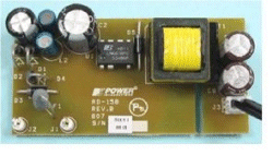
Figure 4 illustrates just how few components are required to produce a highly efficient charger/adapter fully meeting all requirements for EMI, safety, and ruggedness.

Fig. 4. Complete 5-V, 1,000-mA application
Although the design achieves a 6% improvement over the Energy Star EPS v2.0 requirement for a 5-W supply, the ultra-low dissipation of
In the 5-V, 1,000-mA design, Power Integrations has shown how the designer can go far beyond the accepted minimum eco-requirements with a product that is both cost-competitive and simple to manufacture.
Further information may be obtained from www.powerint.com.
References
1. Energy Star EPS Version 2.0 external power supply (EPS) specification effective November 1, 2008. United States Environmental Protection Agency.
2. DI-158 Design Idea. LinkSwitch-II 5 W Charger/Adapter. Power Integrations Inc.
3. LinkSwitch-II Family Energy-Efficient, Accurate CV/CC Switcher for Adapters and Chargers. Power Integrations Inc. ■
Advertisement
Learn more about Power Integrations


