The Cortex-R series of cores from ARM focus on real-time applications. The Cortex-R4 core was commonly used in high-volume, deeply embedded SoC applications such as hard-disk drive controllers, wireless baseband processors, consumer products, and electronic control units for automotive systems. All of the R-series offers deterministic and reasonably quick interrupt response. In 2011 ARM introduced the Cortex-R5 and -R7 cores which were said to have increased efficiency and reliability, and enhanced error management for dependable realtime systems. They implement the ARMv7-R architecture, and include Thumb-2 technology for optimum code density and throughput. They run at up to 800 MHz.

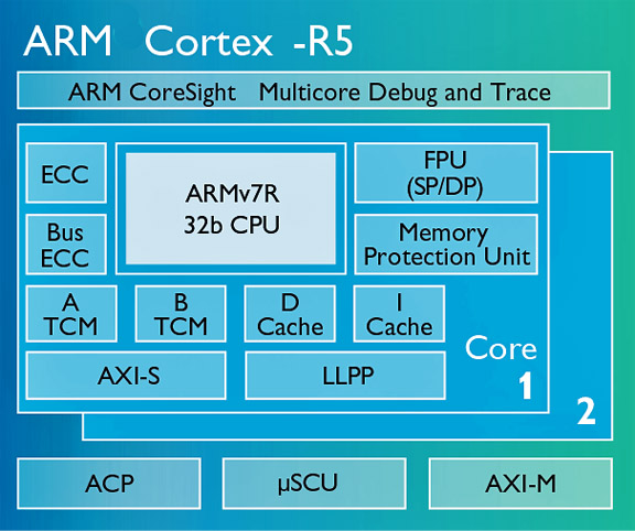
The cores system-level features include a high priority low-latency peripheral port (LLPP) for fast peripheral reads and writes, and an accelerator coherency port (ACP) providing cache coherency for increased data transfer efficiency and more reliable firmware changes. The R5 has about the same basic performance as the R4, while the R7 is, on average, about 45% faster at the same clock speed. The R5 adds dual-core asymmetric multi-processing (AMP) configuration and the R7 has asymmetric or symmetric multi-processing. The two new models add a snoop control unit (SCU) for de-bug. All three have a memory protection unit – the R5/7 with 12 or 16 memory regions. The new cores also add ECC and parity protection to the AXI port bus (as well as the L1 memories).
Interrupt handling
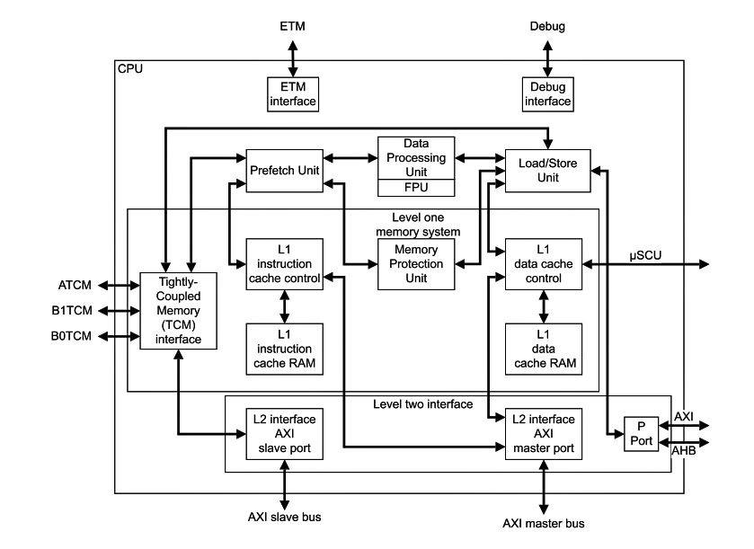
Interrupt latency is kept low by interrupting and restarting load-store multiple instructions, and by use of a dedicated peripheral port that enables low-latency access to an interrupt controller. The processor has Tightly-Coupled Memory (TCM) ports for low-latency and deterministic accesses to local RAM, in addition to caches for higher performance to general memory. Interrupt handling in the processor is compatible with previous designs, but has several additional features for real-time applications.

The core has a dedicated port that enables an external interrupt controller, such as the ARM PrimeCell Vectored Interrupt Controller (VIC), to supply a vector address along with an IRQ. This provides faster interrupt entry, but you can disable it for compatibility with earlier controllers.
On receipt of an interrupt, the processor abandons any pending re-startable memory operations. Restartable memory operations are the multiword transfer instructions LDM, LDRD, STRD, STM, PUSH, and POP that can access normal memory.
To minimize the interrupt latency, ARM recommends that you do not perform:
- multiple accesses to areas of memory marked as Device or Strongly Ordered
- SWP operations to slow areas of memory.
Exception processing
The ARMv7-R architecture contains exception processing instructions to reduce interrupt handler entry and exit time: SRS – Save return state to a specified stack frame; RFE –
Return from exception using data from the stack; and CPS – Change processor state, such as interrupt mask setting and clearing, and mode changes.
Safety processing
Lately, ARM has been touting their safety support for automotive, health, and industrial markets using the Cortex-R5 processor. Their comprehensive safety document set is a huge advantage to engineers and will most certainly drive R5 adoption in safety critical applications. ISO 26262 documentation supports automotive applications such as powertrain and Advanced Driver Assistance Systems (ADAS), while industrial safety-related systems can demonstrate compliance to IEC 61508.
Texas Instruments
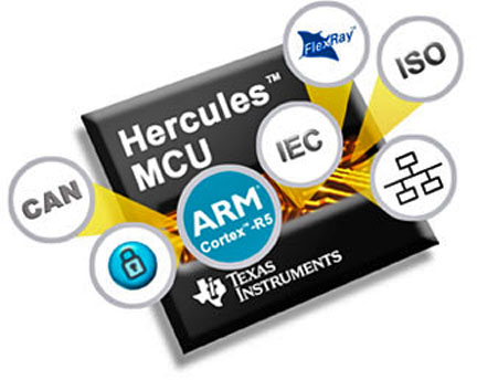
One major R5 implementation is in the Hercules RM57L843 and TMS570LC4357 microcontrollers from Texas Instruments. Very popular for safety applications, especially automotive, they use dual R5s with lock step and up to 4 Mbytes of embedded flash, 512 Kbytes of RAM, dual 12-bit A/Ds, Ethernet, FlexRay, CAN, LIN, and multi-buffered SPI. They run at 330 MHz.

Spansion
The Spansion Traveo microcontrollers are based on the Cortex-R5F core and will deliver high performance, enhanced human-machine interfaces, high-security, and advanced networking protocols tailored for a broad range of automotive applications such as electrification, body electronics, battery management, automotive cluster displays, HVAC, and ADAS.
The family supports the latest in-car networks, and offers high performance graphics engines optimized for a minimum memory footprint, with embed dedicated features to increase data security in the car. The first series of the family, the Traveo MB9D560, features dual ARM Cortex-R5 cores and operates at 200 MHz.
Xilinx
New on scene is the Zynq UltraScale+ MPSoC FPGA family from Xilinx. This device has quad 64-bit Cortex-A53 cores and dual Cortex-R5 real-time cores for heterogeneous multi-processing. The devices use TSMC 16 nm FinFET process technology for an approximately 5X boost in performance/watt. The family also includes a new interconnect optimization technology, SmartConnect, plus a 466 MHz Mali-400M graphics engine and DDR3 and DDR4 external memory interfaces.
Each of the R5 cores has 32 KB of L1 instruction and data cache with ECC protection and 128 Kbytes of tightly coupled memory interface for real-time single cycle access. The processors also have a dedicated interrupt controller and can operate in either split or lock-step mode. In split mode they run independently of each other. In lock-step mode, they run in parallel, with integrated comparator logic, and the TCMs are used as 256 Kbytes of unified memory. The realtime processors (R5) communicate with the rest of the system via the 128-bit AXI-4 ports connected to the low power domain switch. They also communicate directly with the pipeline through these ports. To support real-time debug and trace each core has an Embedded Trace Macrocell (ETM ) that communicates with the ARM CoreSight debug system.
Advertisement
Learn more about ARMSpansionTexas InstrumentsXilinx


