There have been a surprising number of improvements in plain old standard passives in recent years, and articles in this issue will point out some of them. We have higher performance in inductors with higher current ratings for a given size because of improved core material. We also get much better tantalum capacitors. The size of a 100-μF 6.3-V tantalum/tantalum polymer capacitor has come down from 100 mm3 to as low as 9.8 mm3 in the last 8 to 10 years — without a lot of fanfare, so you may not have really noticed.
One of the major contributors to ESR in a capacitor is the second electrode, where the conventional tantalum capacitor uses MnO2 . In tantalum polymer capacitors it is replaced by an organic material: conductive polymer. This leads to a significant reduction of ESR, especially at frequencies above 100 kHz. Typically the ESR value is reduced by about a quarter.
As of today, conventional tantalum technology usually offers the highest capacitance in a given case size, but both polymer and NbO technologies are moving toward higher CV faster and will provide an equivalent solution in the near future.
It seems to me that circuit design engineers are, in the pretty near future, going to turn into system design engineers. Almost all components will be integrated into silicon and EEs will select from various functional modules and some software IP to make up a system — fully simulated, of course.
Higher integration is the name of the game. For now, this focuses on ESD/EMI protection, LED ESD/TVS protection, RF-matching devices, and mixed signal integrated filter modules. STMicroelectronics, for example, uses advanced semiconductor technologies to integrate commonly used circuit elements such as passive filters, ESD suppressors, and wireless baluns in a much smaller size than discrete solutions. As semiconductor devices, ST's components also display tighter tolerances and higher stability than conventional discrete components for accelerated time to market and improved quality.
An example of integration that has been around for some time is the power supply in package or power supply on chip (PwrSoC). Wafer level magnetics (WLM) take magnetic components from their three-dimensional discrete shape to a planar two-dimensional thin-film form that can be deposited using standard wafer processes on top of CMOS wafers. One good example product here is the EN6360QI from Enpirion (recently acquired by Altera) — an 8-A 96%-efficient dc/dc buck converter with integrated inductor in a 8 x 11 x 3-mm QFN package. The complete power system-on-a chip has a total footprint of just 190 mm2 , while showcasing excellent power efficiency over the entire operating temperature range.

The tiny EN6360QI 0.6 to 5.8-V 8-A power converter integrates power transistors, inductor, and gate drive in a tiny package.
The device integrates power switches, electroplated wafer level magnetics, gate drive, controller, and loop compensation and gives the designer a complete power system that is fully simulated, characterized, and production qualified.
You may be familiar with 3D and 2.5D chip technology. These two methods allow for silicon die interconnect using TSV (through-silicon vias). The 3D stacks two or more die on top of each other with interconnect using the TSVs. The 2.5D puts two or more die on a silicon “interposer.” The interposer has no transistors on it — it has all the TSVs. TSVs can have various artifacts the can make life a little difficult in stacked die 3D systems, such as thermal expansion etc. Putting all the TSVs on the interposer means you can have the advantages of the TSV interconnect without the complexity of mixing them with transistors.
Eric Beyne is the program director, 3D integration at imec in Leuven, Belgium. He and his group know just about everything about 3D stacking and interposers. Their research has found that 3D is actually the less expensive way to go — if you have the right methodology. They have developed the Costar Software Tool to optimize the 3D stacked IC test flow, taking into account the yields and costs of design, manufacturing, packaging, testing, and logistics.

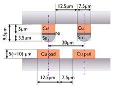
20-μm-pitch μBump interconnects for silicon interposer.
But, notes Eric, the interposer in the 2.5D method is a great place to integrate passive components, especially I/O and power filter R/C/L components. These would be made using semiconductor methods, not as solder-down separate SMT devices, and could have big production and reliability advantages.
Advertisement
Learn more about Electronic Products Magazine


