How THD, placement, and performance can be used
to optimize the fidelity of the audio path
BY ENRIQUE O. RODRIGUEZ
Fairchild Semiconductor
South Portland, ME
www.fairchildsemi.com
As consumers increasingly use their mobile phones to listen to their music collections, the demand for high-end audio quality increases. For many mobile phone audio engineers this means the adoption of various audio techniques that deliver the best sound possible. At the back end of their designs is the routing of these high-quality audio signals to the headphones.
In many cases, multiple sources “feed” the audio amplifier through analog switches but designers always must understand the fidelity of the full audio path from the codec to the headphones. This article will explain the subtleties of audio analog switches and how total harmonic distortion (THD), placement, and performance can be used to optimize the fidelity of the audio path.
A typical mid-to-high-end mobile phone design has multiple sources of audio from the baseband, application processor or standalone audio codec. Although many of the phones are designed for a tailored function such as the music in phones, different signals may be routed based on the function. These signals include left and right audio when talking on the phone generated by the baseband or listening to an MP3 file that would be generated from the application processor.
The end result is the same where multiple audio signals would be routed to the audio jack. The routing of these signals would be implemented via most likely an analog audio switch. Depending on the input to the switch it would either be a dc biased signal or an ac (or negative swing) coupled signal. In many cases the dc level of the signal will dictate what analog switch is required, either a negative swing for ac signals or a standard audio switch.
Once the placement of the analog switch has been determined, the primary routing component to consider is a low RON switch. The reason is that for audio signals the resistance of the analog path will contribute to the power losses of the overall system. If you think of the audio routing path and the load as a simple voltage divider, lowering the RON of the audio path results in less power lost as heat in the system and more power delivered to the headphones. This is especially critical when you are trying to drive low impedance headphones.
Typically most high-performance audio switches will be around the 0.4-Ω range. Most new designs have the input signals of the analog switch to be negative swing or ac biased because it removes the large 220-µF dc blocking capacitors and allows for lower cost of material and simplified designs. This is consistent with the ongoing trend of cap-free audio amplifiers. A number of companies have these negative-swing analog switches, but only Fairchild Semiconductor has a portfolio, including the FSA2269 and FSA2271 that removes the traditional charge pump architecture in order to save power. These devices are dual SPDT for routing of left and right signals to an audio connector. This translates to tens or hundreds of microamperes in savings.
THD
Next, an audio engineer will always measure the total harmonic distortion (THD) of the respective components. Traditionally the rule of thumb THD requirement for audio amplifiers has been 0.1%. Although this is sufficient for audio amplifiers, the audio engineer needs to budget the THD of the entire audio path, which can end up being in the 1% range, which is still not audible to the “common” human ear. So if we consider the audio path from the baseband processor to the headset including all of the components such as the PCB, amplifiers, analog switches and headphones the total THD should be less than 1%. We must consider the analog audio switch THD based on the voltage supply in order to determine the optimal audio THD to be compliant with the 1% range.
THD is inherently related to the on-resistance of the analog switch. Traditionally as on-resistance increases, on-resistance flatness, or the variation in on-resistance across the input voltage, also increases. This increase in on-resistance flatness degrades THD performance. The flatter the on-resistance across the voltage input the better THD performance. A common on-resistance flatness for an audio analog switch such as the FSA2271 is around 0.4 Ω at a 3-V supply for the input voltage range. Typically the on-resistance flatness will vary with the supply voltage; this can be seen in Fig. 1 .
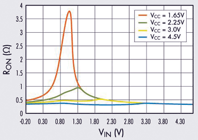
Fig. 1: RON flatness vs. input voltage. (THD results are for a 1-Vpp signal with a 1-V offset driving a 32-Ω load.)
Figure 1 shows a low 0.4-Ω negative swing switch that varies over supply voltage and the effects on the on-resistance. As we can see at 1.65-V supply voltage the RON spikes well over 3.5 Ω at ~1-V VIN, but if we take the THD at this supply voltage it would translate to a THD of over 4% as seen in Fig. 2 .
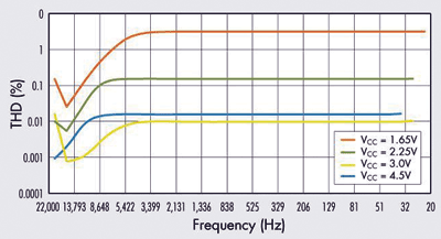
Fig. 2: THD vs. frequency.
For a high-fidelity system, a supply voltage of 1.65 V for a specified negative swing switch would completely disrupt the performance. This is to say that even though a lot of focus is placed on the high-performance audio amplifiers, understanding how to apply analog audio switches becomes critical to an audio engineer. If a designer were to utilize an audio amplifier with low THD and then feed the signal to an analog switch that was at the high THD supply voltage it would completely degrade the system and performance of the audio signal.
If we look closer to Fig. 2 , we would determine that the lowest THD for the system is actually at 3.0-V supply for this particular switch. This is surprising, since at 4.5 V we actually get higher than 0.01% THD. Although this is relative to the specific analog switch being tested, the lesson still remains that when selecting or applying an audio analog switch, one must make sure to fully understand the audio THD of the switch at the various supply voltages. This will only help the performance of the total audio path.
One of the last things to consider for an audio analog switch is the crosstalk between the disconnected throw and the common port since the baseband processor can send audio while the application processor sends audio as well. Some audio architectures will actually “bleed” the audio signal to the common port, which will corrupt the headphone audio signal. This is possible in a number of situations, even when the analog switch is not powered up and can leak the signal to the headphones, otherwise known as power-off protection. So when selecting the proper analog audio switch make sure to understand whether or not the device has power-off protection and off-isolation in order to maintain your audio quality. As an example the FSA2271T has off-isolation (OIRR) and crosstalk (Xtalk) specifications of 70 dB at 100 kHz. Some analog switches such as the FSA2271T also have termination resistors used for ensure that the unselected ports are discharged to ground helping to remove some of the audio “click and pop.”
As we have seen from this discussion, selecting an audio analog switch to fit the needs of the system can be made simple as long as the critical parameters are considered. Even in a portable device, understanding and managing the effects of all components in the audio path will provide improved system performance and ensure robustness of the overall design. ■
Advertisement
Learn more about Fairchild Semiconductor


