By Matt Guibord, systems engineer, high-speed converters, Texas Instruments
As high-speed analog-to-digital converters (ADCs) have increased in sampling rate, so has the problem of code errors — also known as sparkle codes — in the ADC’s output data. A code error is defined as an error in the output code of an ADC that exceeds a defined threshold. The threshold is most commonly defined as the level where an error exceeds the expected amplitude of the ADC’s noise such that the error can be easily identified in the presence of noise.
Another way to explain this definition of the error threshold is that the error amplitude occurs with a probability exceeding the expected probability of that amplitude given the ADC’s assumed Gaussian distributed noise. Fig. 1 shows an example code error found in the output samples of an ADC. The erroneous sample is clearly visible when compared to the ideal sine wave fit and far exceeds the noise of the other samples in the plot.
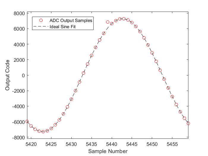
Fig. 1: Example of an ADC output with a code error.
An ADC’s code error rate (CER), also sometimes called word error rate (WER) or metastability error rate, is defined as the average number of errors per sample and is measured by counting the average number of samples between consecutive errors. It is most often defined as an order of magnitude, such as 10–12 errors/sample. The average time between errors, therefore, depends on the sampling rate of the converter. The measured CER is accurate only when the ADC is running at the sampling rate at which the CER was measured. In general, reducing the sampling rate can improve the CER by orders of magnitude.
Let’s take a look at where code errors come from to see why sampling rate is a major factor.
What makes an ADC sparkle?
A multistep ADC architecture, such as a pipelined flash ADC or a successive approximation register (SAR) ADC, converts the sampled voltage to digital bits in stages, and each consecutive stage relies on the result of the previous stage. Consider a basic pipelined flash high-speed ADC, as shown in Fig. 2 . This simplified ADC shows two conversion stages wherein each successive stage produces a digital code that more finely estimates the input signal.
The operation of the shown ADC is as follows:
- The first stage samples the input voltage and coarsely converts the analog input signal to a digital code using the first-stage ADC. The flash ADC in this stage works by comparing the sampled voltage against static voltage references, generated from the ADC’s main reference voltage (VREF ), using high-speed comparators. The output of the flash comparators is a thermometer-encoded digital sample representing the input voltage.
- The converted thermometer code is then sent directly to the first-stage DAC. This DAC outputs the analog voltage, which corresponds to the coarsely converted sample.
- Subtracting the output of the first-stage DAC from the original input voltage results in the quantization error voltage or residue voltage (VRES ). The residue is then amplified and resampled (pipelined) for the second stage.
- The second-stage ADC quantizes VRES to obtain a more accurate (higher-resolution) estimate of the original analog input voltage.
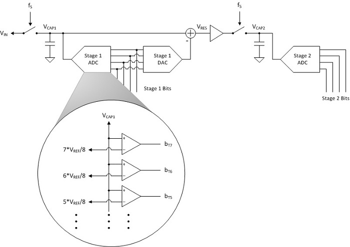
Fig. 2: Example of a pipelined flash ADC architecture block diagram.
The VRES creation process introduces a high-speed decision loop. Within one sampling clock period, the sampled voltage must be converted to a digital code by the first-stage ADC. The digital code must be output from the first-stage DAC, subtracted from the original input voltage and resampled by the second stage. The high-speed decision loop introduces code errors because the comparator in the flash ADC has a settling time that is a function of the difference between the sampled voltage and VREF .
More simply, a comparator takes longer to settle when the input voltage (VCAP1 ) is close to the reference voltage (such as 7 * VREF /8) of the comparator. Theoretically, if VCAP1 is infinitesimally close to the comparator’s reference voltage, the comparator will never settle because it will be operating in its linear region.
Noise will prevent this from actually occurring, but if the comparator does take too long to settle, then the first-stage DAC may use the incorrect digital code to output the quantized analog voltage. The result is a VRES that doesn’t match the first-stage ADC’s actual digital output code. The second-stage ADC then converts the wrong VRES , which results in a code error.
What affects CER?
You should now have enough detail to be able to draw some conclusions on what affects the CER. The CER clearly depends on the sampling rate. A faster sampling rate reduces the time in which the decision loop has to make a decision. Less time to make a decision results in exponential increases in the probability that the comparator has not settled in time.1 Also note that the speed of the comparator directly affects the CER, which is a strong function of the process technology in which the ADC is built. A third factor is the architecture of the ADC.
Multistep architectures with high-speed decision loops are susceptible to poor CER. There are techniques used to reduce CER for these architectures, such as using faster process technologies, implementing time interleaving, or employing asynchronous clocking.2, 3 On the other hand, architectures that do not use high-speed decision loops, such as the folding-interpolating architecture, can use multiple comparator relatch stages without affecting any following stages to greatly reduce the probability of metastability.4
Single-step architectures, therefore, have inherently better CER against comparable pipelined flash or SAR ADC architectures. Multistep architectures with decision loops cannot use comparator relatching without corresponding speed reductions.
An example of the impact of code errors
Let’s look at an example of how code errors may impact an oscilloscope measurement. Assume that an RS-485 transmitter is intermittently outputting a glitch, and the engineering team is trying to measure that glitch on an oscilloscope in order to find the root cause. Suppose that the glitch is small, occurs once every few days, and the oscilloscope uses a simple voltage threshold detection. Also assume that the oscilloscope is sampling at 10 GSPS and has a code error rate of 10–12 errors/sample. Are you more likely to catch the glitch from the transmitter or find a code error from the ADC? Let’s find out!
The mean time between errors in seconds is Te , which you can calculate from the CER and ADC sampling rate (fS ), according to Equation 1:
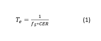
Taking the RS-485 glitch example from above, the mean time between errors for the oscilloscope is calculated as 100 seconds. If the RS-485 glitch occurs every few days, then it will be quite difficult to capture the desired glitch from the device under test because the oscilloscope will be consistently triggering on the code errors.
So what CER would be acceptable? Table 1 shows the mean time between errors for various error rates and sampling rates. At 10 GSPS, a code error rate of much less than 10–15 will be required to capture a glitch that occurs every few days. An oscilloscope built using a folding interpolating ADC, such as the ADC12DJ5200RF , would have a very high likelihood of catching the glitch without an intermittent code error causing a false trigger because of its low CER of 10–18 .

Table 1: Te versus CER and sampling rate.
Code errors have varying degrees of impact on high-speed ADC applications. Oscilloscopes and pulse-based time-of-flight (ToF) systems (such as LiDAR or laser distance measurement) may be more sensitive to code errors when using simple threshold detection, whereas communications or radar systems may be less sensitive.
Communications systems, for instance, often make use of forward error correction (FEC), which can overcome the effect of a single code error in the ADC sample data. Radars use a matched filter (correlation)-based detection algorithm that uses long waveforms to improve detection accuracy, which inherently mitigates the impact of a single code error.
Code errors in the frequency domain
The frequency spectrum of a code error, as seen in the output of a discrete Fourier transform (DFT), is a raised noise floor of equal value at all frequency bins. The calculation below starts from the definition of the normalized DFT, with output Xk , to the output spectrum when a code error is present, Yk . The

term present in Yk is the frequency contribution of a single code error represented as an impulse in the time domain signal. The noise-floor power for a real DFT is raised by

which is proportional to the code-error amplitude squared, α2 , and inversely proportional to the length of the DFT squared, N2 . Therefore, systems that use longer signal lengths or analysis windows will see less of an impact from code errors.
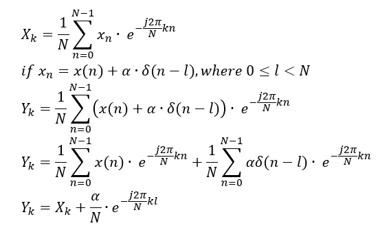
Fig. 3 illustrates the raised noise floor caused by the code error in Fig. 1 , which has an amplitude of 758 codes. The resulting noise power per bin for a real DFT of length 65,536 is calculated to be –110.98 dBFS/bin after normalizing the result to the full-scale power of a 14-bit converter,

This result matches the measured noise floor in the plot of Fig. 3 that is corrupted by the code error.
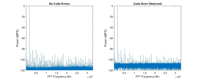
Fig. 3: Frequency domain with and without a code error.
Conclusion
Code errors manifest as unwanted impulses in the time-domain output of high-speed ADCs . In the frequency domain, measured using a DFT, a code error results in a raised noise floor. While some applications can live with these code errors, others, such as oscilloscopes or pulse-based ToF, require a low error rate to be successful.
Code errors are a result of comparator metastability in multistep ADC architectures that require high-speed decisions in the previous stage to occur quickly in order for the next stage to use the result. Sampling rate, comparator speed, and ADC architecture affect the CER of an ADC design.
ADC architectures that do not require high-speed decision loops, such as the folding-interpolation architecture, have inherently better CER due to their ability to relatch the comparator outputs, reducing the probability of metastability without corresponding speed reductions.
The ADC12DJ5200RF , an ultra-high-speed ADC, offers the lowest available CER in the industry and enables engineers to achieve high measurement confidence for test and measurement applications.
References:
1 B. Zojer, R. Petschacher and W.A. Luschnig, “A 6-Bit/200-MHz Full Nyquist A/D Converter,” IEEE Journal of Solid-State Circuits SC-20, no. 3 (June 1985): 780–786.
2 B. Razavi, “Design Considerations for Interleaved ADCs.” IEEE Journal of Solid-State Circuits 48, no. 8 (August 2013): 1,806–1,817.
3 L. Kull, T. Toifl, M. Schmatz, P.A. Francese, C. Menolfi, M. Brandli et al. “A 3.1 mW 8b 1.2 GS/s Single-Channel Asynchronous SAR ADC with Alternate Comparators for Enhanced Speed in 32 nm Digital SOI CMOS.” IEEE Journal of Solid-State Circuits 48, no. 12 (December 2013): 3,049–3,058.
4 R.C. Taft, P.A. Francese, M.R. Tursi, O. Hidri, A. MacKenzie, T. Hoehn et al. “A 1.8V 1.0GS/s 10b Self-Calibrating Unified-Folding Interpolating ADC with 9.1 ENOB at Nyquist.” San Francisco, California: IEEE International Solid-State Circuits Digest of Technical Papers (2009): 78–80.
Advertisement
Learn more about Electronic Products MagazineTexas Instruments


