Op amps and ADCs specify key parameters differently
BY JIM KARKI
Texas Instruments, Dallas, TX
www.ti.com
High-performance A/D converters (ADCs) used in wireless base stations, high-speed data acquisition, test and measurement, medical imaging, and military applications require high-performance differential-input-drive circuits. Designing the drive circuit for optimum spurious free dynamic range (SFDR) and signal-to-noise ratio (SNR) from the ADC is a key challenge for the design engineer.
ADC characterization
A typical test set up for characterization, as shown in Fig. 1 , locks the clock and input signal phase and uses narrow band filters. This allows coherent sampling to obtain the best noise and linearity performance.
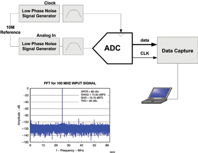
Fig. 1. ADC characterization sets a baseline for maximum ADC performance
The ADC input circuit often uses back-to-back transformers to change the single-ended inputs to differential with best phase and amplitude balance. To build a comprehensive database of SNR and SFDR versus input signal frequency and sampling rate, many filters are required. ADC characterization is optimized to achieve the best possible device performance. Actual implementation in a design is usually a compromise of development time and cost, versus allowable degradation of data sheet specifications. Real designs typically require amplification of the input signal and some type of fixed bandwidth filter.
Op amps vs ADCs
Operational amplifier (op amp) SNR can be computed by first calculating the output (spectral density) noise using the input referred noise, gain and resistor values. To obtain the total rms noise, integrate the output noise over the filter’s equivalent noise bandwidth between the op amp and ADC. SNR is then calculated by taking 20*log10 of the ADC’s input full scale divided by the band limited total rms noise from the op amp.
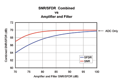
Fig. 2. How SNR and SFDR combine, given an ADC with an SNR and SFDR specification of 70 dB and increasing amplifier with filter performance.
The equivalent amplifier specification to SFDR is distortion: harmonic distortion for single tone, and inter-modulation distortion for multitone. The performance varies depending on gain, output amplitude, frequency and load. A datasheet should include plots to show these variations, but interpolation may be required to attain your desired condition.
For example, your design might require distortion at 10 MHz and 3 Vp-p in a gain of 10, while the data sheet plots a gain of one distortion versus frequency at 2 Vp-p, and distortion versus output amplitude and gain at 5 MHz. To estimate performance for your conditions, take the value shown for gain of one with 2 Vp-p at 10 MHz and subtract the difference between 2 and 3 Vp-p for 5 MHz, as well as the difference between a gain of one and a gain of 10 for 5 MHz.
Combining amplifier and ADC SNR and SFDR performance metrics
Next, estimate the overall system performance by combining the SNR and SFDR metrics for the amplifier and ADC, using Equation 1.
facn_TexasInsequation1_nov2010 Equation 1
SNR is always added in RMS fashion, like power:
If the ADC and amplifier plus filter SNRs are equal; the overall SNR is 3 dB less than the ADC. With higher SNR performance from the amplifier and filter, the SNR asymptotically approaches that of the data converter. A 0.1 dB degradation is achieved when the amplifier and filter are optimized for 15 dB better SNR than the ADC.
SFDR calculations are less straightforward. When combining tones or harmonics of tones from two different sources, the phase between the sources significantly impacts the resultant. When they are in-phase, they add linearly (1+1=2). When they are 180˚ out-of-phase, they cancel one another out (1-1=0). Other phase relationships fall somewhere in between. Also, only the same type of spurs can be combined, such as second harmonic from the amplifier and second harmonic from the ADC. If we assume an in-phase relationship, the worst case is computed on a spur-by-spur basis to determine the spur that will set the SFDR, assuming the spur is given as a positive value in dBc, not negative value as is commonly used for distortion. See Equation 2:

Equation 2
If the ADC and amplifier plus filter spurs are equal, the overall spur is 6 dB worse than the ADC. With higher spur performance from the amplifier and filter, the combined performance asymptotically approaches that of the ADC. A 1-dB degradation is achieved when the amplifier and filter are optimized for 18 dB better performance than the ADC.
The diagram in Fig. 2 shows how SNR and SFDR combine per the equations above, given an ADC with an SNR and SFDR specification of 70 dB and increasing amplifier with filter performance.
Filtering and balance
In a sampled system, such as an ADC, all input frequencies fall in the first Nyquist-zone (0Hz to fSAMPLE/2), and filtering is required for best performance.
Low-pass filters (LPF) are often used when the input frequencies of interest fall within the first Nyquist-zone. When the desired data bandwidth is much less than fSAMPLE/2, a simple-first-order LPF with a resistor and capacitor (RC) is often used. When the data is higher bandwidth, higher order filters – including resistors, inductors, and capacitors (RLC) – can help achieve more aggressive filtering.
In higher-Nyquist-zone sampling applications, bandpass filters (BPF) are required and are usually higher-order RLC filters.
As previously mentioned, all high-performance ADCs use differential inputs. The key reasons are:
1. Better noise rejection.
2. Double the signal amplitude versus single-ended inputs of the same amplitude.
3. Even-order distortion suppression.
Rejecting system noise and effectively doubling the input signal amplitude provide the best SNR performance, while suppression of even-order distortion provides higher SFDR performance.
To achieve the best even-order distortion when filtering a differential signal, balance must be maintained. A mere five degrees of imbalance can cause significant performance degradation.
When using RLC LPFs in first Nyquist applications, place the filter corner frequency above the band of interest to avoid the main phase shifts caused by the filter.
When using RLC BPFs in higher Nyquist applications, the main phase shifts of the filter cannot be avoided because they happen in the passband. In this case, a transformer or balun may be required between the filter and ADC to re-balance the signal.
Architectures for driving differential input ADCs
Signals in systems are often single ended and must be converted to differential for driving the ADC. There are three ways to do this:
1. Transformers or baluns are excellent at converting single-ended inputs to differential. They require no power, add no noise, and are very linear. The turns ratio can be used to step the voltage up or down. They do not pass dc, but many provide a secondary center tap where the ADC input common-mode-bias can be applied. Their primary drawback is flatness versus frequency. Many times an amplifier is still required and radio frequency (RF)-type amplifiers are often used, especially at higher frequencies, but may require high power to achieve low even-order harmonics.
2. Single-ended op amps can be used in various configurations. One suitable for lower frequencies uses a non-inverting op amp to provide the in-phase output, while also driving an inverting op amp to provide the out-of-phase output. The challenge with this architecture is the two outputs are inherently mismatched and balance cannot be maintained as frequency increases.

Fig. 3. An example using the THS770006 op-amp to convert a single-ended input to differential for driving an ADC.
3. Fully differential op amps (FDAs) can take a differential input or convert a single-ended-input to a differential output. FDAs provide a dc-coupled means to convert a single-ended-input to a differential output with better performance at higher frequency than other op-amp solutions, and provide an easy means to set the common-mode input to the ADC. The newest generation of FDAs provide the best performance yet for driving 14- and 16-bit ADCs. Figure 3 shows an example using TI’s THS770006 to convert a single-ended input to differential for driving an ADC. ■
Advertisement
Learn more about Texas Instruments


